Method for the application of a conformal nanocoating by means of a low pressure plasma process

A low-pressure plasma and plasma technology, applied in the field of plasma technology, can solve problems such as complex production processes and achieve cost savings

Inactive Publication Date: 2012-12-12
EUROPLASMA
View PDF9 Cites 40 Cited by
  • Summary
  • Abstract
  • Description
  • Claims
  • Application Information

AI Technical Summary

Problems solved by technology

The production process is complex because of the use of solid precursors that must be sublimed to start, and then pyrolysis must be performed before the formation of useful monomers in the gas phase

Method used


Image

  • Method for the application of a conformal nanocoating by means of a low pressure plasma process
  • Method for the application of a conformal nanocoating by means of a low pressure plasma process

Examples


example 1

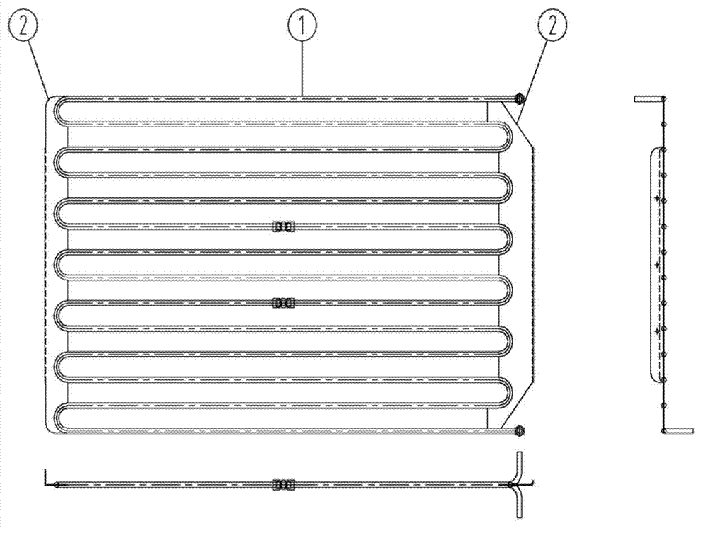
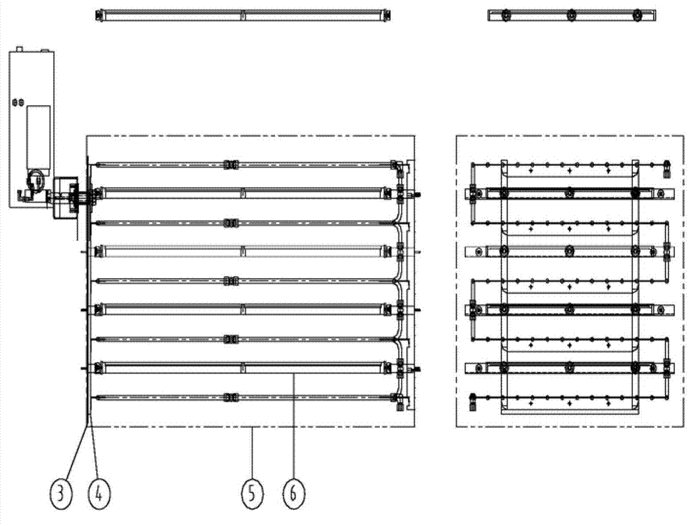
[0049] Example 1: Electrode arrangement in the reaction chamber

[0050] figure 1 with 2 The preferred settings are shown. The electrode set for generating low-pressure plasma includes a set of floating electrodes (1) in a hollow, curved and circular shape and a vacuum chamber (5), and the vacuum chamber (5) is used as the main body. The electrode (1) is provided with a liquid, which can be cooled or heated to perform plasma treatment in a temperature range of 5 to 200°C, and is preferably controlled at a temperature between 20 to 90°C.

[0051] The typical electrode (1) in this setup has a diameter between 5 and 50 mm, a wall thickness of 0.25 to 2.5 mm, and is bent toward the end with a 180° turning circle, and the tube is between before and after bending The distance between is between 1 to 10 times the tube diameter, preferably 5 times.

[0052] Power is applied to the electrode (1) through a connecting plate (2) installed on a clutch plate (4). A thin insulating layer or prot...

example 2

[0056] Example 2: Low-voltage plasma polymerization C3F6 embedded in circuit boards for phones

[0057] The assembled circuit board for the mobile phone was placed in the CD1000 plasma chamber for more than two minutes, as described in Example 1, and was degassed at a pressure between 100 and 1000 mTorr. Then, the board was cleaned and etched with Ar, and plasma polymerization was performed with C3F6 monomer at 50 mTorr and room temperature for 10 minutes. The fluoropolymer conformal coating applied by this process was measured to have a thickness of about 80 nm.

[0058] The board was then exposed to several aging processes, involving extended exposure to moisture, high temperature, and salt fume. It can be seen visually that circuit boards with conformal nano-coatings show significantly lower corrosion than untreated circuit boards. When performing electrical tests, it can also be found that the circuit board assembly with the nano-conformal coating actually shows no electrical...


PUM

PropertyMeasurementUnit
thicknessaaaaaaaaaa
diameteraaaaaaaaaa
thicknessaaaaaaaaaa

Abstract

The invention relates to a conformal nanocoating applied by a low pressure plasma process. The invention also relates to a method for making such a conformal nanocoating on a three-dimensional nanostructure, in particular a three-dimensional structure containing electrically conductive and non-conductive elements.

Description

Technical field [0001] The invention relates to a low-pressure plasma process for conformally applying a nano-coating on a three-dimensional structure. The present invention also relates to the application of such conformal coatings on three-dimensional nanostructures made of different materials, especially on three-dimensional structures containing conductive and non-conductive elements. Background technique [0002] Most electronic devices are mainly three-dimensional structures of conductive materials and electrically insulating materials. Such electronic devices include not only equipment but also components, bare and assembled printed circuit boards (PCB), and individual components such as integrated circuits and transistors. The conductive part of such a structure is usually composed of a metal such as copper, aluminum, silver or gold or a conductive polymer or semiconductor material. The non-conductive parts or insulators of these structures are usually composed of polym...

Claims


Application Information

Patent Timeline
Patent Type & Authority Applications(China)
IPC IPC(8): B05D7/24H05K3/28H01J37/32H01L23/29
CPCH05K2201/015B05D3/0493B05D3/142H01J37/32541H01L2924/09701H05K3/282B05D1/62H05K2203/095H05K2201/09872H05K3/284B05D2506/10H01L2924/12044H01L23/293B05D5/083H01L2924/0002Y10T428/239H01L2924/00B05D7/24H05K3/28H01J37/32H01L23/29
Inventor F.赖盖恩A.范兰德赫姆P.马腾斯
Owner EUROPLASMA
Why Eureka
Try Eureka