
Method for forming metal silicide

A metal silicide and silicon substrate technology, applied in the direction of electrical components, semiconductor/solid-state device manufacturing, semiconductor devices, etc., can solve problems such as increased leakage current, poor quality of metal silicide formation, and increased device resistance

Inactive Publication Date: 2012-12-19
SEMICON MFG INT (SHANGHAI) CORP
View PDF4 Cites 6 Cited by
  • Summary
  • Abstract
  • Description
  • Claims
  • Application Information

AI Technical Summary

Problems solved by technology

[0005] During the formation of metal silicide, attention should also be paid to the influence of the oxide layer on the silicon surface. If there is an oxide layer on the silicon surface, the formation quality of the metal silicide will be poor, resulting in increased device resistance and increased leakage current.

Method used


Image

  • Method for forming metal silicide
  • Method for forming metal silicide
  • Method for forming metal silicide

Examples


Embodiment Construction

[0029] The principles and features of the present invention are described below in conjunction with the accompanying drawings, and the examples given are only used to explain the present invention, and are not intended to limit the scope of the present invention.

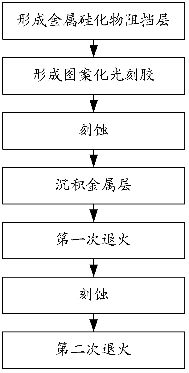
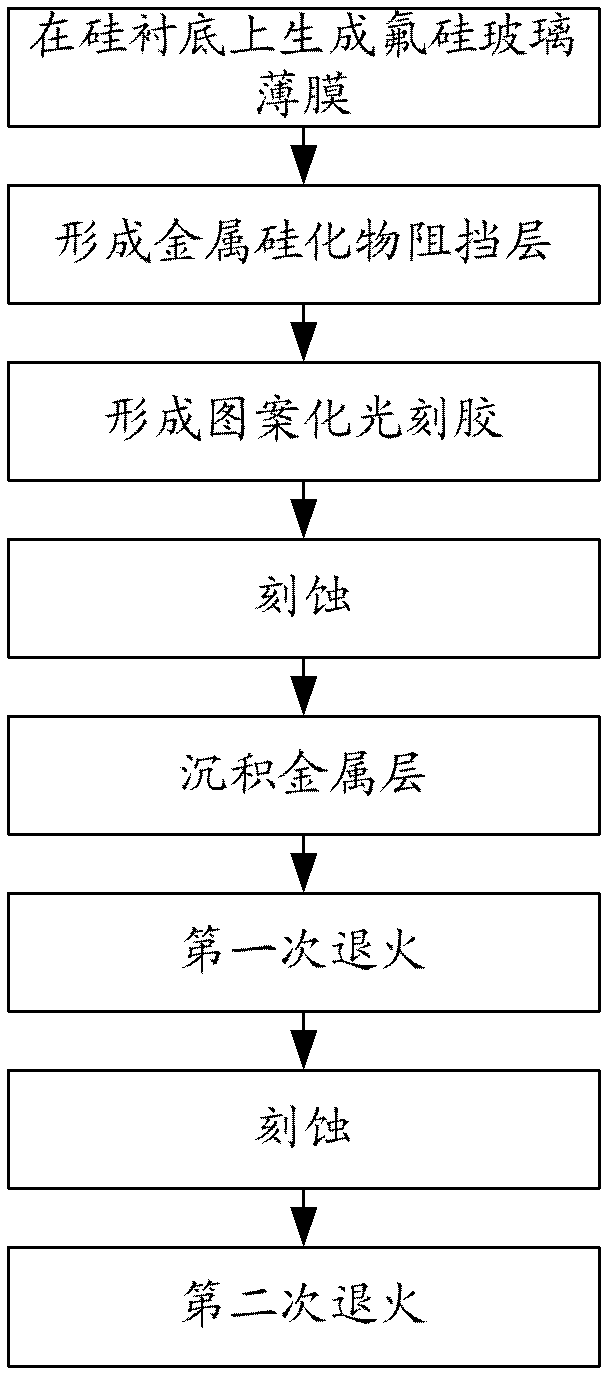
[0030] figure 2 It is a flow chart of a metal silicide forming method of the present invention, such as figure 2 As shown, the main steps of this method include:

[0031] Deposit a layer of fluorosilicate glass film on the silicon substrate as a buffer layer;

[0032] Depositing a metal silicide barrier layer on the fluorosilicate glass thin film buffer layer;

[0033] forming a patterned photoresist on the metal silicide barrier layer corresponding to the predetermined area where the silicide needs to be generated on the silicon substrate;

[0034] Etching by using the patterned photoresist as a mask to expose a predetermined area on the silicon substrate where metal silicide needs to be generated and remove t...


PUM

PropertyMeasurementUnit
thicknessaaaaaaaaaa
thicknessaaaaaaaaaa
thicknessaaaaaaaaaa

Abstract

The invention provides a method for forming metal silicide. Before a metal silicide block layer is formed, a layer of silicofluoride glass film is deposited on a silicon substrate to be as a buffer layer. Fluorine element in the silicofluoride glass film can spread into the silicon substrate. Introduction of the fluorine element can restrain the metal from suddenly entering the silicon substrate together in an initial stage when the metal silicide is formed, and can fix the metal element which has already spread into the silicon substrate, thereby reducing defects.

Description

technical field [0001] The invention relates to the technical field of semiconductor manufacturing, in particular to a method for forming a metal silicide. Background technique [0002] With the rapid development of VLSI, the integration of devices is getting higher and higher, and the size is getting smaller and smaller. When the size of the device is reduced to the sub-micron level, many problems will arise accordingly, such as the metal oxide semiconductor field effect (MOS) transistor, due to the reduced size, it will cause the gate electrode and the source / drain region of the MOS transistor to be damaged. Surface resistance and contact resistance increase, causing signal delay in MOS transistors. [0003] In order to solve the problems caused by reducing the size of the device, the metal silicide process is generally used to deposit refractory metals titanium (Ti), cobalt (Co), Nickel (Ni), etc., form metal silicide through an annealing process, but there are also som...

Claims


Application Information

Patent Timeline
Patent Type & Authority Applications(China)
IPC IPC(8): H01L21/28H01L21/768H01L21/336
Inventor 鲍宇荆学珍平延磊肖海波
Owner SEMICON MFG INT (SHANGHAI) CORP
Learn More