Liquid crystal display device

A liquid crystal display device and liquid crystal layer technology, applied in optics, instruments, electrical digital data processing, etc., can solve the problems of reduced yield, low touch panel sensitivity, display mode limitations, etc. Transmittance, the effect of reducing power consumption

Active Publication Date: 2012-12-26
KUSN INFOVISION OPTOELECTRONICS
View PDF4 Cites 34 Cited by
  • Summary
  • Abstract
  • Description
  • Claims
  • Application Information

AI Technical Summary

Problems solved by technology

Many TFT-LCD manufacturers have invested heavily in this technology, but its technology is limited. Most of them use resistance, capacitance or light sensing. The wiring on the electrode structure is relatively complicated and the yield rate is low. , affecting the aperture ratio, especially poor compatibility with wide viewing angle technology
[0004] For the resistive sensor (Resistive Sensor) method, since the upper substrate must be easy to bend, the density of the main photo spacer (Main Photo Spacer, Main PS) used on the upper substrate is relatively small, and a relatively small force can be used. Make the upper substrate bend, increase the sensitivity, but if the main photo-spacer density is too low, the display quality of the panel will be affected
[0005] For the optical sensor method, its sensitivity is high, but in a relatively dark environment, the sensitivity of th

Method used


Image

  • Liquid crystal display device
  • Liquid crystal display device
  • Liquid crystal display device

Examples


Embodiment Construction

[0032] In order to make the above objects, features and advantages of the present invention more comprehensible, specific implementations of the present invention will be described in detail below in conjunction with the accompanying drawings.

[0033] It should be noted that, for the sake of clarity of illustration, the drawings of the present invention only show structural features related to the inventive point of the present invention, while other structural features are omitted.

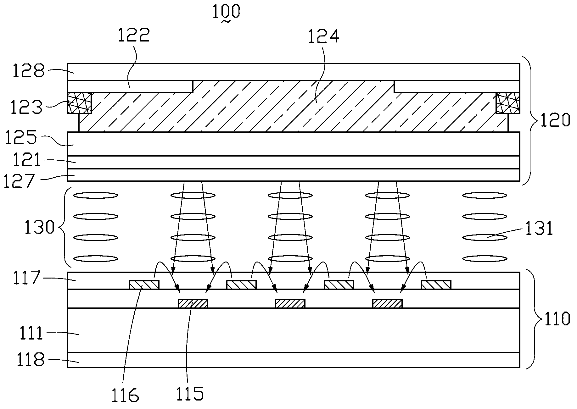
[0034] figure 1 It is a schematic structural diagram of the liquid crystal display device according to the first embodiment of the present invention. Such as figure 1 As shown, the liquid crystal display device 100 of the present invention includes a first substrate 110 and a second substrate 120 disposed opposite to each other, and a liquid crystal layer 130 sandwiched between the first substrate 110 and the second substrate 120 .

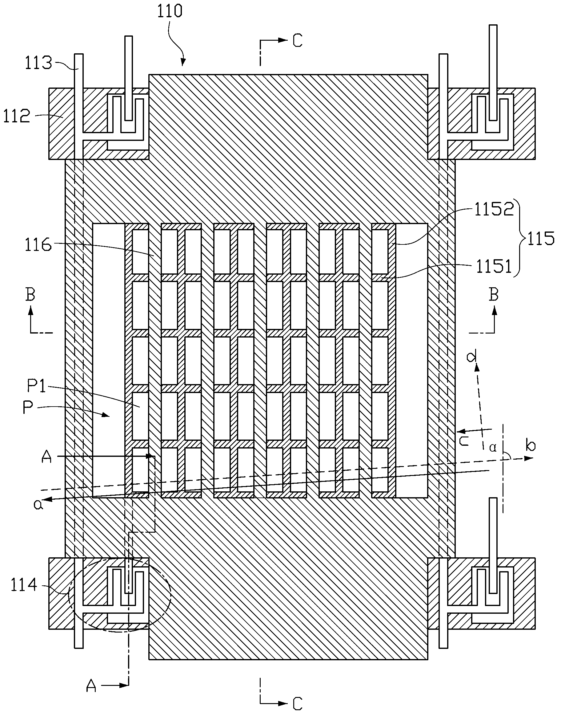
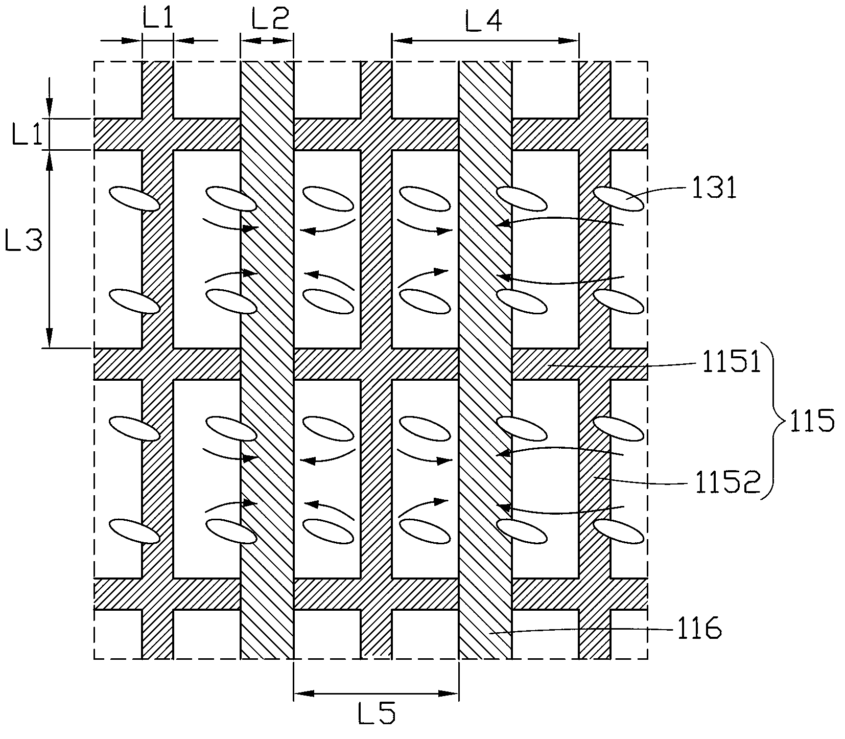
[0035] specifically, Figure 2-3 and Figures 4a-4c reveal...


PUM


Abstract

The invention discloses a liquid crystal display device which comprises a first baseplate, a second baseplate arranged opposite to the first baseplate, and a liquid crystal layer clamped between the first baseplate and the second baseplate, wherein the first baseplate comprises a plurality of scanning lines and a plurality of data cables, which are crossed to one another to define out a plurality of pixel areas; each pixel area is composed of pixel electrodes and a plurality of first public electrodes in electric connection, and the pixel electrodes and the first public electrodes are positioned on different layers; the second baseplate comprises touch-control sensing electrodes, as well as a black matrix and a colour layer both arranged on the touch-control sensing electrodes; and the liquid crystal molecules of the liquid crystal layer are negative liquid crystal molecules. The liquid crystal display device integrates an embedded touch control board technology and a wide visual angle, and has a wider visual angle and higher permeability.

Description

technical field [0001] The invention relates to the technical field of liquid crystal display, in particular to a liquid crystal display device. Background technique [0002] Thin Film Transistor-Liquid Crystal Display (TFT-LCD) is widely used in the field of flat panel display due to its low radiation, thin thickness and low power consumption. Since the principle of LCD is to control the spatial direction of liquid crystal molecules through the electric field and change the vibration direction of the incident light from the backlight, if the screen is viewed from an oblique angle, color distortion may occur, which limits the viewing angle of the LCD. The industry tries to improve the viewing angle characteristics of liquid crystal displays through various technologies. Several wide viewing angle technologies have been proposed, such as MVA (Multi-domain Vertical Alignment, multi-domain vertical alignment) mode, OCB (Optically Compensated Bend / Optically Compensated Birefring...

Claims


Application Information

Patent Timeline
IPC IPC(8): G02F1/1333G02F1/1343G06F3/044
Inventor 钟德镇李永谦廖家德
Owner KUSN INFOVISION OPTOELECTRONICS
Why Eureka
Try Eureka