Optimizing design method of nanometer technical metal layer map

A metal layer and layout technology, applied in the field of optimized design of nano-process metal layer layout, to achieve the effects of improving manufacturability, optimizing area, reducing the amount of data and correction time

A metal layer and layout technology, applied in the field of optimized design of nano-process metal layer layout, to achieve the effects of improving manufacturability, optimizing area, reducing the amount of data and correction time

CN102855360AInactive Publication Date: 2013-01-02INST OF MICROELECTRONICS CHINESE ACAD OF SCI

Image

  • Optimizing design method of nanometer technical metal layer map
  • Optimizing design method of nanometer technical metal layer map
  • Optimizing design method of nanometer technical metal layer map

Examples


Embodiment 1

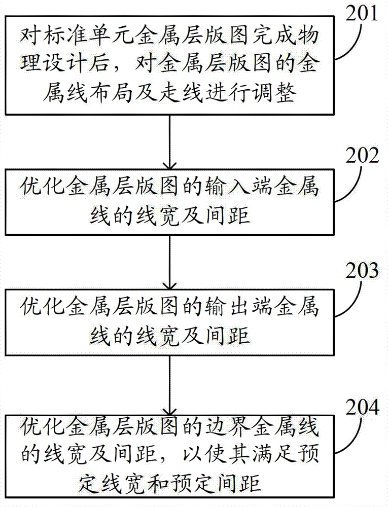
[0047] An embodiment of the present invention provides a method for optimizing the design of a metal layer layout in nanotechnology, the flow chart of which is as follows figure 2 shown, including the following steps:

[0048] Step 201: After completing the physical design of the metal layer layout of the standard cell, adjust the metal line layout and routing of the metal layer layout;

[0049]Specifically, after the physical design of the standard cell metal layer layout is completed, and before the OPC correction process is performed on the metal layer layout, according to the basic principle of OPC correction and the basic structure of the corrected mask pattern, the overall layout of the metal layer layout can be adjusted, The line width, height and spacing of metal lines are optimized.

[0050] Step 202: Optimizing the line width and spacing of the metal line at the input end of the metal layer layout;

[0051] Specifically, the line width of the metal lines at the in...

Embodiment 2

[0063] An embodiment of the present invention provides a method for optimizing the design of a metal layer layout in nanotechnology, the flow chart of which is as follows Figure 4 shown, including the following steps:

[0064] Step 401: reducing redundant corners of metal lines in the metal layer layout;

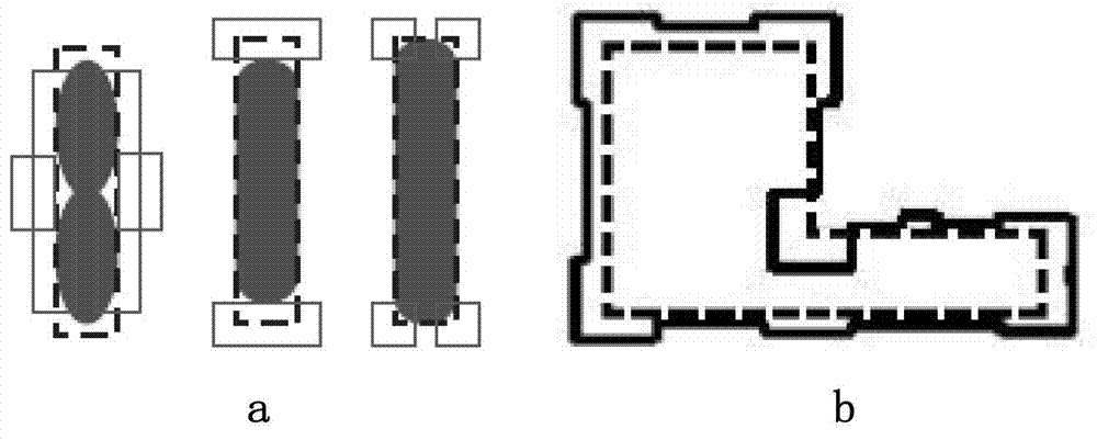
[0065] At the 90° corner of the metal line, due to large distortion due to optical effects, there is a large deviation between the actual graphic and the layout graphic; and for the metal line with multiple corners appearing continuously in a small range, the actual graphic obtained becomes extremely inconsistent. Rules, which affect the manufacturability of the chip, therefore, need to reduce the redundant corners of the metal lines in the metal layer layout.

[0066] Specifically, reducing the redundant corners of the metal lines of the metal layer layout may include the following steps:

[0067] For metal wires connecting multiple MOS tube ports, set the metal wire con...


PUM


Abstract

The embodiment of the invention provides an optimizing design method of a nanometer technical metal layer map. The method comprises the steps as follows: physically designing a standard unit metal layer map, and then adjusting the arrangement and direction of metal lines of the metal layer map; optimizing the width and spacing of the metal lines at the input end of the metal layer map; optimizing the width and spacing of the metal lines at the output end of the metal layer map; and optimizing the width and spacing of the metal lines at the boundary of the metal layer map, so as to meet the preset width and the preset spacing of the metal lines. With the adoption of the optimizing method provided by the embodiment of the invention, the turning in the metal layer map is reduced, and the metal layer map can be uniform in density distribution; the optics proximity correction and modification area required by the metal layer map can be optimized, the data volume in the optics proximity correction and modification and the modification time can be reduced, the manufacturability of a chip is improved, and the manufacturing cost of the chip is saved.

Description

technical field [0001] The invention relates to the technical field of integrated circuit manufacturing, in particular to an optimal design method of a metal layer layout of a nanometer process. Background technique [0002] At the technology node below 90nm, the feature size of the chip is already close to or even smaller than the wavelength of the light wave used in the photolithography process. Therefore, in the lithography process, due to the interference and diffraction effects of light waves, there are certain deformations and deviations between the lithography pattern and the layout pattern on the actual wafer. This error in lithography directly affects the manufacturability of the chip. (Design For Manufacturing, DFM). In order to obtain high-resolution and more realistic layout graphics, optical proximity correction (Optical Proximity Correction, OPC) and other photolithography technologies are applied to the mask manufacturing process. A pattern as close as possi...

Claims


Application Information

Patent Timeline
02 Jan 2013
Publication
CN102855360A
IPC
G06F17/50
Inventors
赵浙业; 陈岚