Storage element, method of manufacturing storage element, and storage device

A storage element and storage layer technology, applied in the direction of electrical components, information storage, static memory, etc., can solve the problems of low operating speed, difficulty in achieving integration, etc., and achieve improved heat resistance, high reliability, and no degradation Effect

Active Publication Date: 2017-03-01
SONY CORP
View PDF8 Cites 0 Cited by
  • Summary
  • Abstract
  • Description
  • Claims
  • Application Information

AI Technical Summary

Problems solved by technology

However, each of these types of memory has advantages and disadvantages
Specifically, flash memory is highly integrated, but not strong in terms of operating speed
FeRAM is difficult to achieve higher integration due to the limitation of microfabrication, and there are also problems in manufacturing process
MRAM has disadvantages in terms of power consumption

Method used


Image

  • Storage element, method of manufacturing storage element, and storage device
  • Storage element, method of manufacturing storage element, and storage device
  • Storage element, method of manufacturing storage element, and storage device

Examples


no. 1 approach

[0030] 1. Storage element (wherein the ion source layer comprises a first ion source layer and a storage element of a second ion source layer)

[0031] 2. Method of Manufacturing Memory Element

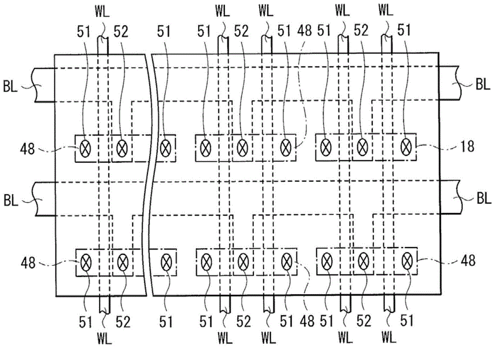
[0032] 3. Storage device

[0033] [Modification]

[0034] [Memory element including two resistance change layers arranged on top of each other]

no. 2 approach

[0036] [Memory element in which the second ion source layer has a multilayer structure]

Embodiment

[0038] [first embodiment]

[0039] [storage element]

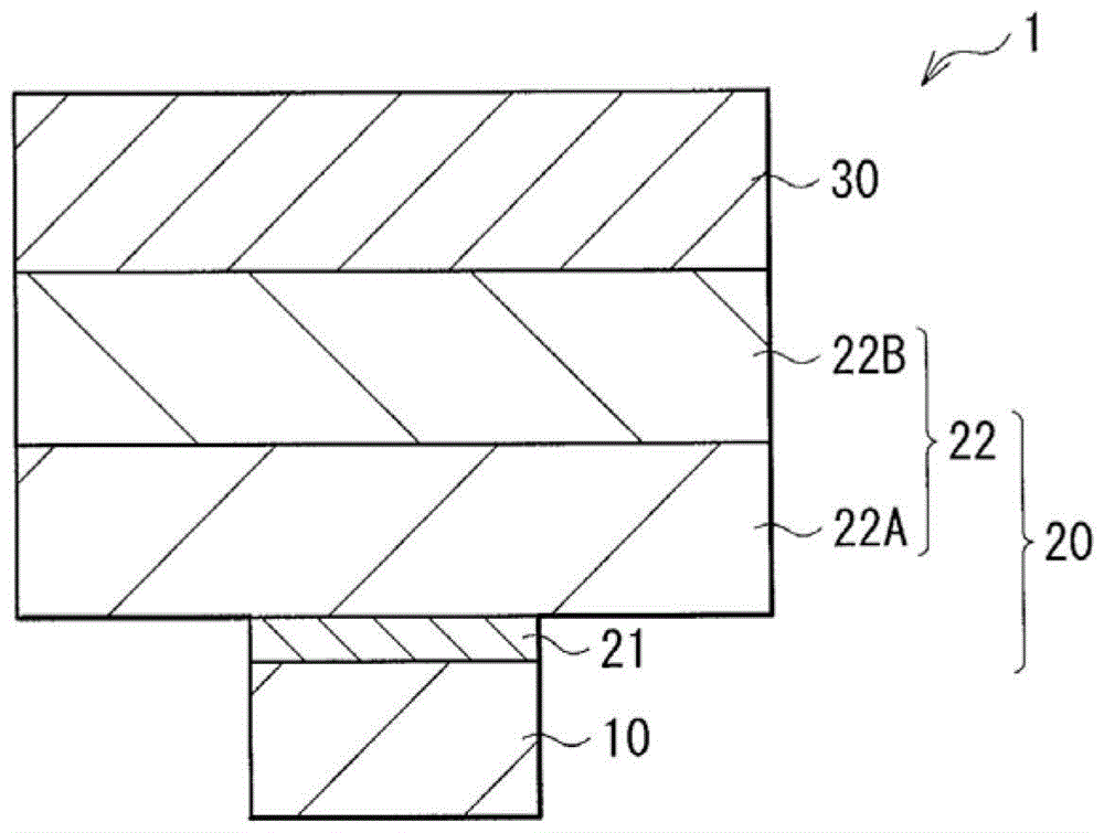
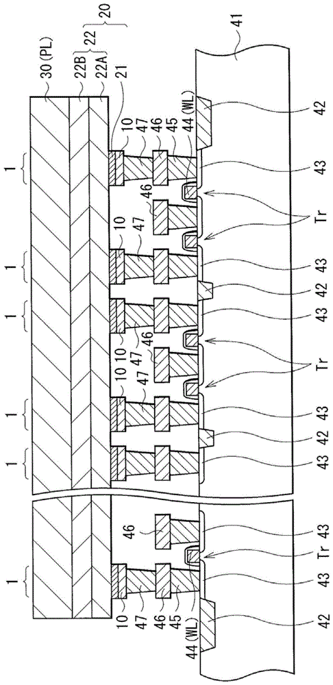
[0040] figure 1 It is a cross-sectional view showing the structure of the memory element 1 according to the first embodiment of the present invention. The memory element 1 sequentially includes a lower electrode 10 (first electrode), a memory layer 20 and an upper electrode 30 (second electrode).

[0041] The lower electrode 10 is provided, for example, on a layer ( Figure 4 ) on the silicon substrate 41 of a CMOS (Complementary Metal Oxide Semiconductor) circuit, thereby serving as a connection portion with the CMOS circuit portion. The lower electrode 10 is made of a material used for wiring in a semiconductor process, such as tungsten (W), tungsten nitride (WN), copper (Cu), aluminum (Al), molybdenum (Mo), tantalum ( Ta) and silicide. When the lower electrode 10 is made of a material that may cause ion conduction in an electric field, such as Cu, the surface of the lower electrode 10 may be covered with a material...


PUM


Abstract

The present invention provides a storage element, a method for manufacturing the storage element, and a storage device, wherein the storage element sequentially includes a first electrode, a storage layer, and a second electrode. The storage layer includes: a resistance change layer disposed on the first electrode side; and an ion source layer containing one or more metal elements, and the ion source layer is disposed on the second electrode side. The ion source layer includes a first ion source layer and a second ion source layer, and the first ion source layer contains more than one of the chalcogen elements tellurium (Te), sulfur (S), and selenium (Se) and is set On the resistance change layer side, and the content of chalcogen elements in the second ion source layer is different from the content of chalcogen elements in the first ion source layer, and the second ion source layer is arranged on the second electrode side . According to the present invention, the ion source layer can be prevented from being deteriorated, and the heat resistance of the memory element is improved. In other words, the formed memory device has high reliability.

Description

[0001] Cross References to Related Applications [0002] This application contains subject matter related to and claims priority from Japanese Patent Application JP2011-146113 filed in the Japan Patent Office on Jun. 30, 2011, the entire content of which is hereby incorporated by reference. technical field [0003] The present invention relates to a memory element that stores information based on any change in electrical characteristics observed in a memory layer including an ion source layer and a resistance change layer, a method of manufacturing the memory element, and a memory device. Background technique [0004] In information equipment such as computers, widely used random access memory is DRAM (Dynamic Random Access Memory) with high operating speed and high density. However, the manufacturing cost of the DRAM is high due to the complicated manufacturing process of the DRAM compared to a logic circuit LSI (Large Scale Integration) or a signal processing circuit gener...

Claims


Application Information

Patent Timeline
Patent Type & Authority Patents(China)
IPC IPC(8): G11C13/00H01L45/00
CPCG11C13/0011G11C2213/55G11C13/0007H10B63/82H10B63/30H10N70/245H10N70/8416H10N70/826H10N70/8828H10N70/8833H10N70/231
Inventor 紫牟田雅之保田周一郎水口徹也大场和博荒谷胜久
Owner SONY CORP
Why Eureka
Try Eureka