Efficient photoetching manufacturing method of ferrite base membrane circuit

A production method and technology of thin film circuits, which are applied in the direction of circuit, pattern surface photolithography process, semiconductor/solid-state device manufacturing, etc., can solve the problems of difficulty in realizing large-scale equipment production, poor process stability, and low yield rate. Achieve the effect of increasing thickness, strong performance and improving yield

Inactive Publication Date: 2013-01-02
中国电子科技集团公司第九研究所
View PDF5 Cites 2 Cited by
  • Summary
  • Abstract
  • Description
  • Claims
  • Application Information

AI Technical Summary

Problems solved by technology

[0004] The problem to be solved by the present invention is: to overcome the deficiencies in the prior art, to provide a microwave ferrite thin film circuit device (such as isolator/circulator) manufacturing technolog

Method used


Image

  • Efficient photoetching manufacturing method of ferrite base membrane circuit
  • Efficient photoetching manufacturing method of ferrite base membrane circuit
  • Efficient photoetching manufacturing method of ferrite base membrane circuit

Examples


Embodiment Construction

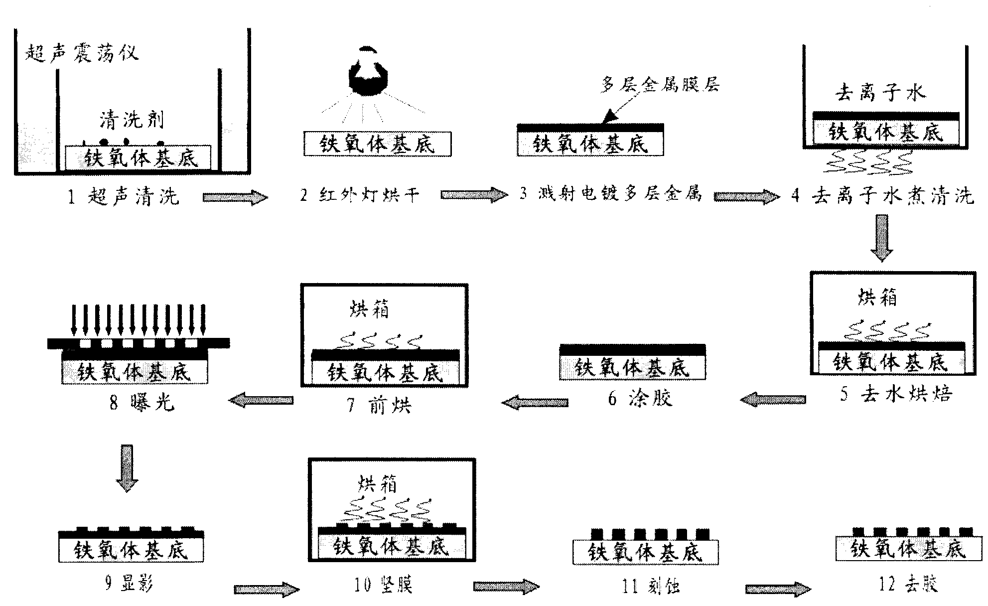
[0020] The method will be described in detail below in conjunction with specific implementation methods and accompanying drawings, but the scope of protection of the present invention is not limited to the following examples, and should include all content in the claims. Moreover, those skilled in the art can realize all the content in the claims from the following embodiment.

[0021] The specific process of this method embodiment is as follows:

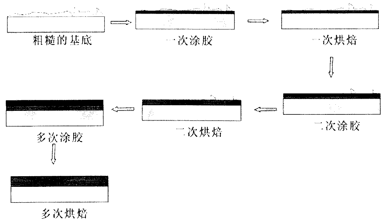
[0022] (1) Select a suitable ferrite substrate material according to the expected preparation of the device, and metallize, clean and dry the substrate. The ferrite substrate needs to be strictly cleaned before sputtering plating, so that the metal film layer is firmly attached to the substrate. The substrate with the metal film before photolithography also needs to be cleaned and removed to prevent the photoresist from being firmly attached to the substrate. , floating glue and other phenomena appear, the drying process needs to s...


PUM

PropertyMeasurementUnit
Thicknessaaaaaaaaaa

Abstract

The invention provides an efficient photoetching manufacturing method of a ferrite base membrane circuit. The efficient photoetching manufacturing method comprises the steps of: (1) selecting a proper ferrite base material according to the requirement of a prepared device as expected; carrying out metalizing, washing and drying on a base; (2) repeatedly gluing and baking the ferrite base which is cleaned and coated with a metal membrane layer, so as to obtain an uniform and dense slushing compound layer which can well protect metal at the bottom layer on a ferrite base sheet; (3) exposing and developing the baked slushing compound to obtain a circuit pattern of the slushing compound; and (4) transmitting the circuit pattern of the slushing compound on the metal through using a wet etching way or dry etching way, so as to achieve the manufacture of the ferrite base micro-strip membrane circuit. The invention provides a method for repeatedly gluing and baking a ferrite base, and therefore, the coated slushing compound layer is uniform and is good in compactness, and the problem that the slushing compound is hardly uniformly coated during photoetching due to the shortcomings that the ferrite base is coarse, porous and the like can be solved; the probability that a pin hole, a sand hole and the like are generated can be reduced, and thus, the steps of manually repairing the pattern in the conventional ferrite membrane circuit manufacture technology can be removed; and as a result, the technological stability and the manufacture efficiency of a ferrite base membrane device can be greatly improved.

Description

technical field [0001] The invention relates to a high-efficiency photolithographic manufacturing method of a microwave oxygen substrate film circuit, which belongs to the category of micro-processing technology. Background technique [0002] Microwave ferrite thin film circuit devices (such as isolators / circulators) are widely used in the field of microwave communications. Due to their advantages of small size, light weight, less consumables, and easy integration, they are widely used in communication stations, satellites, radars, etc. It plays an important role in civilian and military equipment. Market research results show that for a long period of time in the future, the demand for microwave ferrite thin film circuit devices (such as isolators / circulators) will increase day by day. How to prepare ferrite with high efficiency, low cost and reliability Thin-film circuit devices are one of the technical bottlenecks that need to be solved urgently to meet the increasingly ...

Claims


Application Information

Patent Timeline
IPC IPC(8): H01L21/70G03F7/00G03F7/16
Inventor 张为国倪经陈学平李杨兴周俊王喜生曹照亮
Owner 中国电子科技集团公司第九研究所
Why Eureka
Try Eureka