An Enhanced Switching Device

A switching device and enhanced technology, applied in the field of enhanced switching devices and their manufacturing, can solve problems such as device stability and reliability impact, achieve the effects of good compatibility, avoid device performance degradation, and simple manufacturing process

Active Publication Date: 2016-04-13
ENKRIS SEMICON
View PDF4 Cites 0 Cited by
  • Summary
  • Abstract
  • Description
  • Claims
  • Application Information

AI Technical Summary

Problems solved by technology

However, in the existing process, no matter whether it is to reduce the thickness of the nitride barrier layer under the gate, or to keep a layer of p-type nitride under the gate, or to implant negative ions in the barrier layer, it will be affected due to process problems. The stability and reliability of the device have a relatively large impact

Method used


Image

  • An Enhanced Switching Device
  • An Enhanced Switching Device
  • An Enhanced Switching Device

Examples


Embodiment Construction

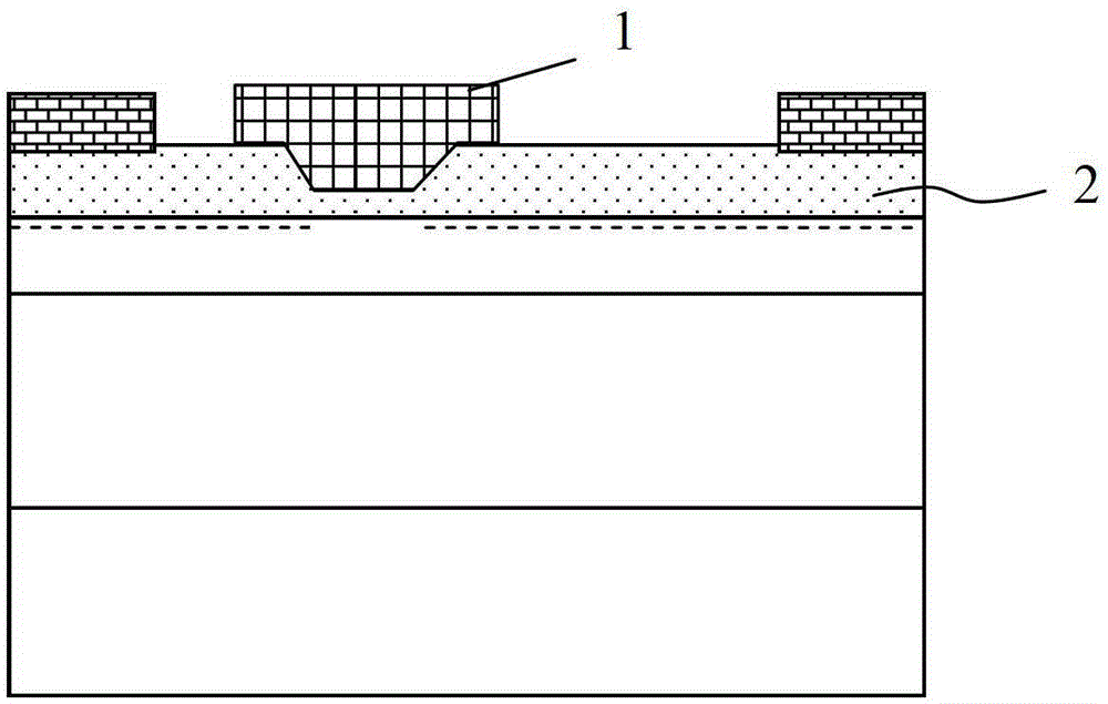
[0042] GaN is a semiconductor material with extremely strong self-built electric field due to spontaneous polarization and piezoelectric effect. Therefore, in the GaN heterojunction structure grown in the polarization direction, a two-dimensional electron gas with a high electron concentration can be generated without intentional doping. However, for the non-polar or semi-polar surface of the gallium nitride material, since there is almost no or very low polarization field strength, two-dimensional electron gas will not be generated without doping. Taking advantage of this characteristic of gallium nitride material, in the present invention, we introduce a non-planar stepped structure in the gate region to generate a non-polar or semi-polar surface of gallium nitride, avoiding the two-dimensional electrons in the gate region. Gas generation, thus realizing the enhanced device.

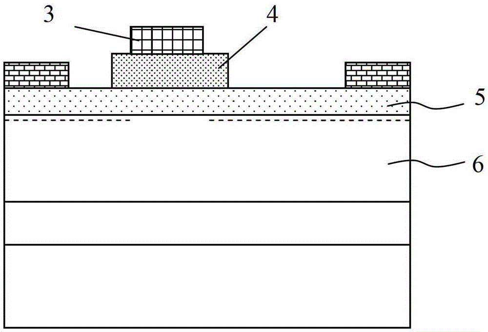
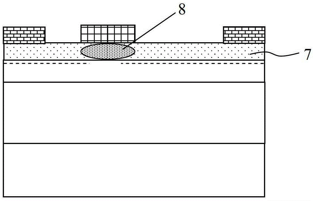
[0043] The embodiment of the present invention discloses an enhanced switching device, including: ...


PUM


Abstract

An enhanced switched device. By introducing a non-planar step-shaped structure in a gate region and generating a gallium nitride non-polar surface, semi-polar surface, or combination thereof, two-dimensional electronic gas is interrupted in the gate region. When the gate voltage increases, an electrically conductive trench if formed in the trench layer, thereby enabling the operation of the enhanced device. The manufacturing technique for the device is simple and is compatible with the manufacturing techniques of conventional depletion type devices.

Description

technical field [0001] The invention belongs to the technical field of semiconductors, and in particular relates to an enhanced switching device and a manufacturing method thereof. Background technique [0002] The third-generation semiconductor material gallium nitride has the characteristics of large band gap, high electron saturation drift velocity, high breakdown field strength, and good thermal conductivity. In terms of electronic devices, gallium nitride materials are more suitable than silicon and gallium arsenide. Manufacture high temperature, high frequency, high voltage and high power semiconductor devices. [0003] Due to the strong two-dimensional electron gas in the AlGaN / GaN heterostructure, usually the AlGaN / GaN HEMT is a depletion device, making it difficult to realize an enhancement device. However, the application of depletion devices has certain limitations in many places. For example, in the application of power switching devices, enhanced (normally off)...

Claims


Application Information

Patent Timeline
Patent Type & Authority Patents(China)
IPC IPC(8): H01L29/778H01L29/10H01L29/423
CPCH01L29/42316H01L29/0657H01L29/2003H01L29/42356H01L29/7786H01L29/7789
Inventor 程凯
Owner ENKRIS SEMICON
Why Eureka
Try Eureka