High-purity Cu bonding wire
A high-purity, lead-in technology, used in electrical components, circuits, electrical solid devices, etc., can solve problems such as excellent hardness, inability to draw circuits, and IC chip cracks
- Summary
- Abstract
- Description
- Claims
- Application Information
AI Technical Summary
Problems solved by technology
Method used
Image
Examples
Embodiment 1
[0044] [Manufacturing method of copper lead for ball bonding]
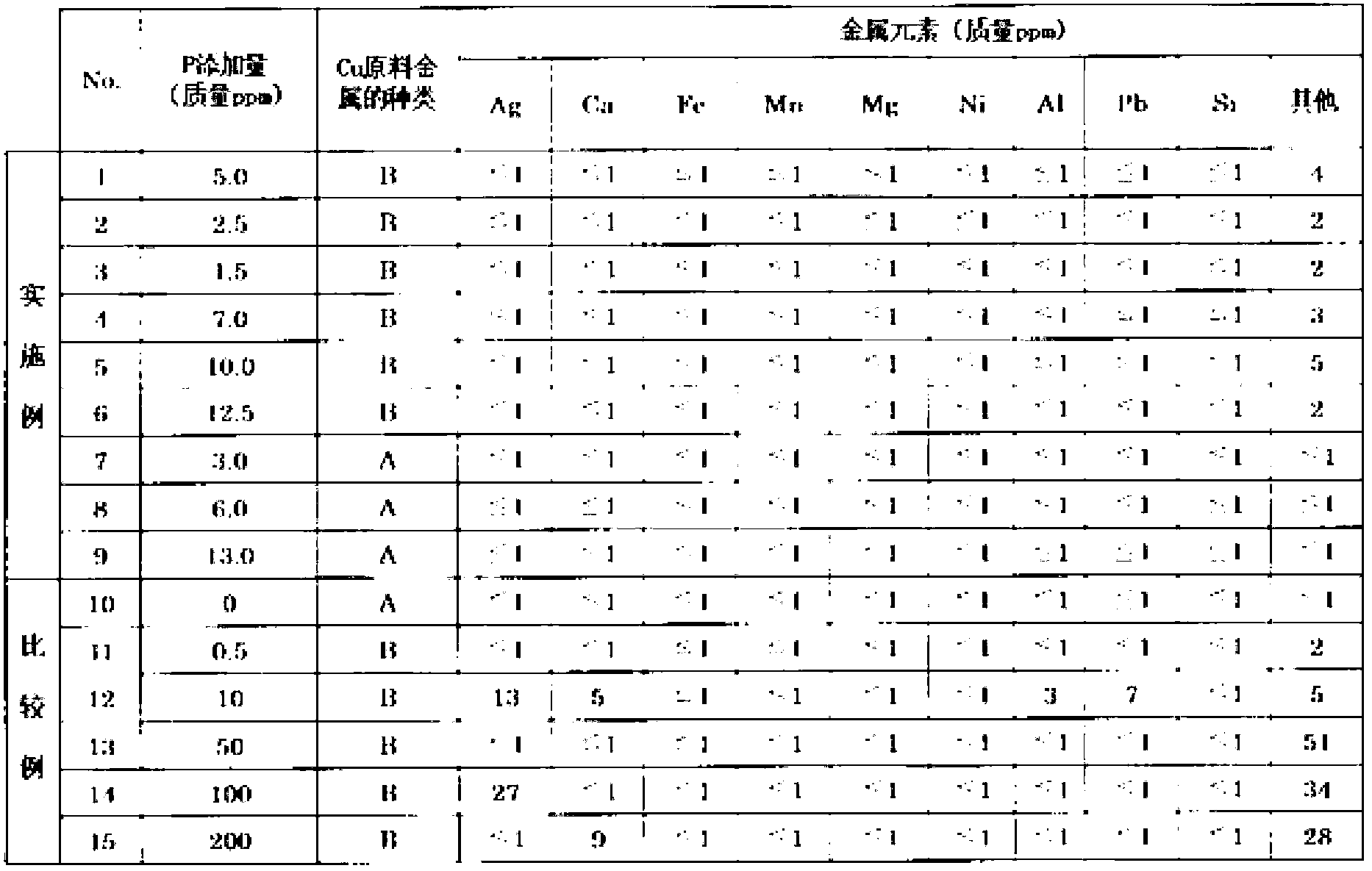
[0045] A method of manufacturing the copper alloy lead for ball bonding according to the present invention will be described. Prepare to add high-purity copper (Cu) metal of 99.9999 mass% or more (as Cu raw material metal [A]) and 99.999 mass% or more of high-purity copper (Cu) metal (as Cu raw material metal [B]) Specimens having copper alloy lead compositions shown in Table 1 containing a predetermined amount of phosphorus (P) were used. Samples with these compositions were processed into soldered leads in the same manner as the method for producing high-purity gold leads. First, a predetermined amount of raw material is melted in a vacuum melting furnace and cast into an ingot. This ingot was rolled with a groove roll and subjected to debonding treatment, antirust treatment, etc., to produce a high-purity copper alloy lead wire with a diameter of 25 μm.
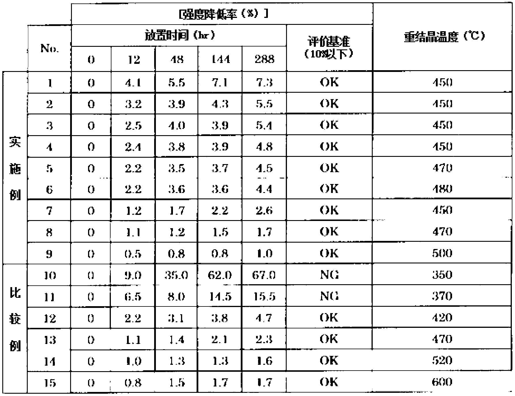
[0046] [Confirmation of aging softening effect]
[0...
PUM
| Property | Measurement | Unit |
|---|---|---|
| Diameter | aaaaa | aaaaa |
Abstract
Description
Claims
Application Information


