Photoelectrochemical method for separating p-type silicon micro-channel from substrate

A photoelectrochemical, p-type silicon technology, applied in the field of photoelectrochemistry, can solve the problems of lack of surface flatness, unfavorable processing, silicon wafer damage, etc., and achieve the effect of high aspect ratio, low cost, and avoidance of damage

Active Publication Date: 2013-01-16
EAST CHINA NORMAL UNIV +1
View PDF3 Cites 12 Cited by
  • Summary
  • Abstract
  • Description
  • Claims
  • Application Information

AI Technical Summary

Problems solved by technology

According to the existing information, physical grinding and polishing are easy to cause damage to the silicon wafer, resulting in a decrease in the structural strength of the microchannel, which is not conducive to subsequent processing; while plasma etching is relatively expensive, and chemical backside thinning is mainly performed by using KOH solution. The backside is etched to expose the silicon microchannels, but due to the anisotropic corrosion characteristics of the alkaline solution, the surface flatness is lacking

Method used


Image

  • Photoelectrochemical method for separating p-type silicon micro-channel from substrate
  • Photoelectrochemical method for separating p-type silicon micro-channel from substrate
  • Photoelectrochemical method for separating p-type silicon micro-channel from substrate

Examples


Embodiment 1

[0043] The method of separating the p-type microchannel from the silicon substrate by increasing the current is as follows:

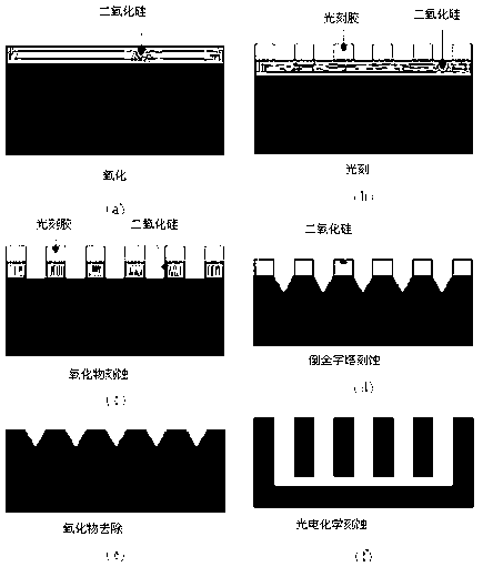
[0044] 1. Select a p-type silicon wafer with a (100) crystal orientation of 7 degrees, and a resistivity of 2-5Ω*cm;

[0045] 2. Using thermal oxidation to form silicon dioxide as a mask;

[0046] 3. Define the window (2um*2um) array by lithography, and define the window through the steps of development, primer, and silicon dioxide removal;

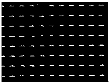
[0047] 4. Put the silicon wafer with the defined window into tetramethylammonium hydroxide (TMAH 80°C) to corrode, and take it out from time to time and watch it under the microscope until a clear cross is seen, as in figure 2 As shown in , the silicon wafer is a silicon wafer engraved with an inverted pyramid structure at this time;

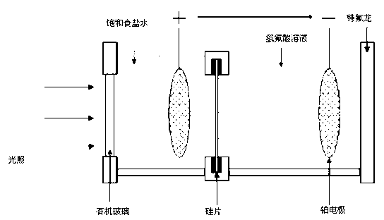
[0048] 5. Put the silicon wafer engraved with the inverted pyramid into the etching tank, install the device, pour 2M hydrofluoric acid etching solution, set the total etching cur...

Embodiment 2

[0051] The method of separating the p-type microchannel from the silicon substrate by reducing the voltage is as follows:

[0052] 1. Select a p-type silicon wafer with (100) crystal orientation, and the resistivity is 2-5Ω*cm;

[0053] 2. Using thermal oxidation to form silicon dioxide as a mask;

[0054] 3. Define the window (2um*2um) array by lithography, and define the window through the steps of development, primer, and silicon dioxide removal;

[0055] 4. Put the silicon wafer with the defined window into tetramethylammonium hydroxide (TMAH 80°C) to corrode, and take it out from time to time and watch it under the microscope until a clear cross is seen, as in figure 2 As shown in , the silicon wafer is a silicon wafer engraved with an inverted pyramid structure at this time;

[0056] 5. Put the silicon wafer engraved with the inverted pyramid into the etching tank, install the device, pour 2M hydrofluoric acid etching solution, set the etching current to 510mA, and se...


PUM

PropertyMeasurementUnit
electrical resistivityaaaaaaaaaa

Abstract

The invention relates to the technical field of micro-electro-mechanical systems, and discloses a photoelectrochemical method for separating a p-type silicon micro-channel from a substrate. The method comprises the following steps: preprocessing positions and figures defining etching points until the etching points have inverted pyramid structures; vertically deeply etching to obtain the micro-channel; and adjusting the size of an etching voltage or an etching current to form transverse etching in order to realize the separation of the micro-channel with the substrate. The peeling of the silicon micro-channel from the silicon substrate through the utilization of the photoelectrochemistry in the invention avoids damages of physical polishing to the silicon micro-channel and damages of chemical corrosion to the silicon surface, so p-type macro-porous silicon (also called micro-channel) having a random depth within 300mum can be prepared.

Description

technical field [0001] The invention belongs to the technical field of micro-electromechanical systems, and in particular relates to a photoelectrochemical method for separating a p-type silicon microchannel from a substrate. Background technique [0002] Porous silicon (porous silicon PS) is a material formed by anodic dissolution of silicon in HF solution. The formation of porous silicon was first reported in the 1950s when studying the electrochemical polishing of silicon. According to the classification standard of the International Union of Pure and Applied Chemistry (IUPAC) for porous silicon, porous silicon can be divided into three types according to the size (width or diameter) of the pores: those larger than 50nm are called macroporous pores. ), those between 2-50nm are called mesoporous, and those with a size smaller than 2nm are called micropores. The size of the pores of the microchannel structure studied in the present invention is generally at the micron (um...

Claims


Application Information

Patent Timeline
Patent Type & Authority Applications(China)
IPC IPC(8): B81C1/00
Inventor 王连卫彭波波王斐赖佳顾林玲王振
Owner EAST CHINA NORMAL UNIV
Why Eureka
Try Eureka