Method for preparing high k-gate dielectrics on surface of graphene by utilizing water-based atomic layer deposition technology

An atomic layer deposition, graphene surface technology, used in coatings, metal material coating processes, semiconductor/solid-state device manufacturing, etc., can solve the problems of depositing high-k gate dielectric layers, lack of thin-film dangling bonds, etc., to improve wetting. performance, improved uniformity and coverage

Inactive Publication Date: 2013-01-23
FUDAN UNIV
View PDF3 Cites 16 Cited by
  • Summary
  • Abstract
  • Description
  • Claims
  • Application Information

AI Technical Summary

Problems solved by technology

[0006] The purpose of the present invention is to propose a method for preparing a high-k gate dielectric on the surface of graphene, to solve the problem that the surface of graphene is hydrophobic and lacks the dangling bonds required for film growth, and it is difficult to directly deposit high-k gates on its surface by ALD process. Medium layer and other issues

Method used


Image

  • Method for preparing high k-gate dielectrics on surface of graphene by utilizing water-based atomic layer deposition technology
  • Method for preparing high k-gate dielectrics on surface of graphene by utilizing water-based atomic layer deposition technology
  • Method for preparing high k-gate dielectrics on surface of graphene by utilizing water-based atomic layer deposition technology

Examples


Embodiment Construction

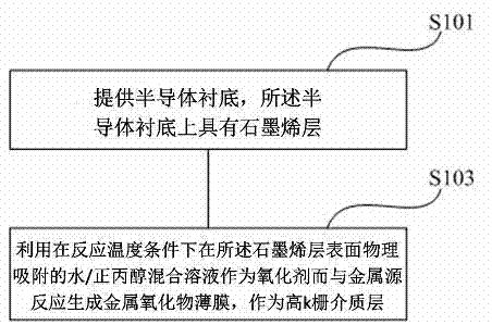
[0028] The inventors of the present invention have found that in the prior art, the oxide gate dielectric layer prepared on the surface of graphene has problems such as poor uniformity and coverage or damage to the crystal structure of graphene, which affects subsequent products (such as graphene-based field effect transistor) device performance.

[0029] Therefore, in the case of graphene-based field-effect transistors, in order to prevent the generation of the above-mentioned defects, the inventors of the present invention have improved the prior art and proposed a novel preparation method for graphene-based field-effect transistors, which mainly utilizes The amphiphilic properties of n-propanol can reduce the surface tension of water physically adsorbed on the graphene surface, thereby improving the wettability between the chemical source and graphene, thereby improving the uniformity and coverage of the metal oxide film deposited on the graphene surface .
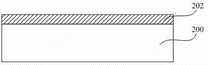
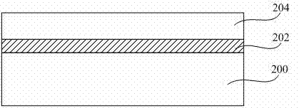
[0030] First, ...


PUM

PropertyMeasurementUnit
thicknessaaaaaaaaaa
thicknessaaaaaaaaaa

Abstract

The invention belongs to the technical field of the manufacturing of a semiconductor device, in particular to a method for preparing high k-gate dielectrics on the surface of graphene by utilizing a water-based atomic layer deposition technology. The method comprises the following steps of providing a semiconductor substrate, wherein a graphene layer which is not functionalized is arranged on the semiconductor substrate; and adopting water / normal propyl alcohol mixed solution physically absorbed on surface of the graphene layer as oxidant to be reacted with a metal soruce to generate a high k-gate dielectric film under the condition of a reaction temperature. The high k-gate dielectric film is one of IIIA-group metal oxide, IIIB-group rare earth oxide and IVB-group transitional metal oxide and any one of binary or more than binary oxides of the IIIA-group metal, the IIIB-group rare earth and the IVB-group transitional metal. Compared with the prior art, the uniformity and the coverage rate of the high k-gate dielectric film which is deposited on the surface of the graphene can be remarkably improved, the structure of the graphene crystal is not damaged in the film deposition process, and the preparation of high-performance graphene device can be facilitated.

Description

technical field [0001] The invention belongs to the technical field of semiconductor device manufacturing, and in particular relates to a method for preparing a gate dielectric on a graphene surface. Background technique [0002] According to Moore's Law, the integration level of chips doubles every 18 months to 2 years, that is, the processing line width is reduced by half. The development path to extend Moore's Law by utilizing the shrinking size of silicon-based semiconductor materials (the processing limit of silicon materials is generally considered to be 10 nanometer line width) is gradually approaching the end. With the continuous reduction of device size in the field of microelectronics, silicon material is gradually approaching its processing limit. [0003] In order to prolong the life of Moore's Law, the international semiconductor industry has proposed Beyond Silicon technology (Beyond Silicon), among which the most promising graphene came into being. Graphene,...

Claims


Application Information

Patent Timeline
Patent Type & Authority Applications(China)
IPC IPC(8): H01L21/285C23C16/40
Inventor 张有为仇志军陈国平陆冰睿刘冉
Owner FUDAN UNIV
Why Eureka
Try Eureka