
Electric device package

A technology for electrical components and packages, applied in the field of electrical component packages, can solve the problems of thermal damage, burnout, electrode thermal damage, etc. of the organic EL layer, and achieve the effect of ensuring the degree of freedom of design

Inactive Publication Date: 2013-01-23
NIPPON ELECTRIC GLASS CO LTD
View PDF6 Cites 17 Cited by
  • Summary
  • Abstract
  • Description
  • Claims
  • Application Information

AI Technical Summary

Problems solved by technology

Therefore, if no thermal countermeasures are taken against the irradiation heat of the laser, the electrode located at the lower part of the glass frit will be unduly heated by the irradiation heat of the laser, causing thermal damage, and sometimes even burning out.
In addition, when the electrodes are heated in this way, the heat is conducted to the organic EL layer through the electrodes, which may cause thermal damage to the organic EL layer.

Method used


Image

  • Electric device package
  • Electric device package
  • Electric device package

Examples


Embodiment 1

[0140] First, the first invention will be described in detail based on examples. In addition, the 1st invention is not limited at all by the following Examples. The following examples are merely illustrations.

[0141]

[0142] Table 1 shows the design values ​​of the film structures of Examples (No. 2 to No. 4) of the dielectric multilayer film used in the electric device package of the first invention. In addition, in Table 1, a single-layer dielectric film is shown as a comparative example (No. 1).

[0143] [Table 1]

[0144]

[0145] Although the dielectric multilayer film with the film structure shown in Table 1 is a simulation, it shows Figure 5 The wavelength characteristics of reflectance as shown. As shown in the figure, compared with the example (No. 2) of the 3-layer structure, the wavelength characteristic of the reflectance becomes better as the number of layers increases, and in the example (No. 5) of the 9-layer structure, the maximum reflectance The ...

Embodiment 2

[0147]

[0148] Table 2 shows an example of the film structure of Examples (No. 6 to No. 8) of the dielectric multilayer film used in the electrical component package of the first invention.

[0149] [Table 2]

[0150]

[0151] The frequency characteristic of the reflectivity of this embodiment (No.6~No.8) is as follows Figure 6 shown. The reflectance of the embodiment (No.7) composed of 6 layers and the embodiment (No.8) composed of 8 layers both reached the maximum near the wavelength of 808nm, and in the embodiment (No.8) composed of 8 layers A maximum reflectivity of about 70% is achieved.

Embodiment 3

[0153]

[0154] After printing a paste-like glass frit with a thickness of 15 μm by screen printing on the peripheral portion of a glass substrate with a length of 40 mm x a width of 50 mm x a thickness of 0.5 mm, pre-firing is performed at 500° C. for 1 hour to temporarily cure the glass frit. Fabricate the sealing substrate.

[0155] Here, as the glass frit, a material containing 99% by mass of inorganic powder and 1% by mass of pigment was used. The inorganic powder contained in this glass frit contained 60 vol% of SnO-based glass powder and 40 vol% of refractory filler. SnO-based glass powder contains 59% SnO, 20% P in mole % 2 o 5 , 5% ZnO, 15% B 2 o 3 , 1% Al 2 o 3 Composition as glass. In addition, the average particle size D of the glass powder 50 2.5μm, the largest particle size D max is 7 μm. The refractory filler is composed of zirconium phosphate powder, with an average particle size of D 50 2μm, the largest particle size D max is 8 μm. On the other ...


PUM

PropertyMeasurementUnit
thicknessaaaaaaaaaa
thicknessaaaaaaaaaa
particle sizeaaaaaaaaaa

Abstract

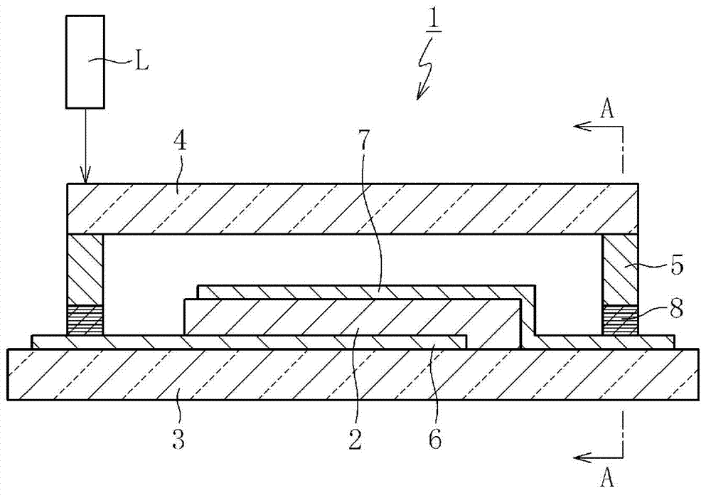
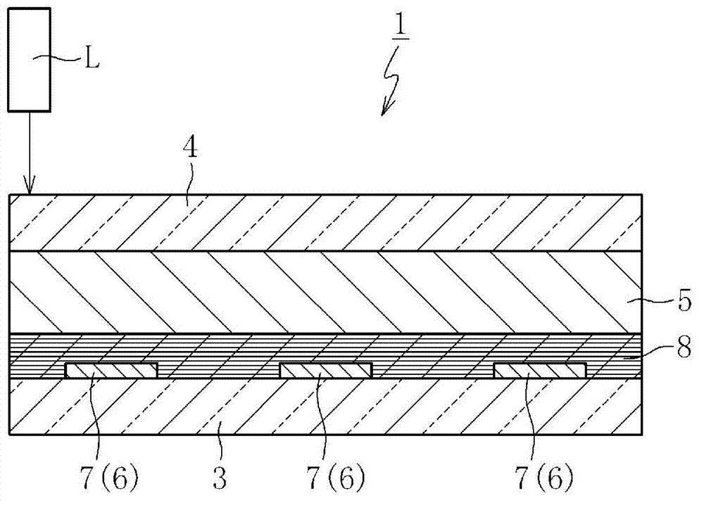
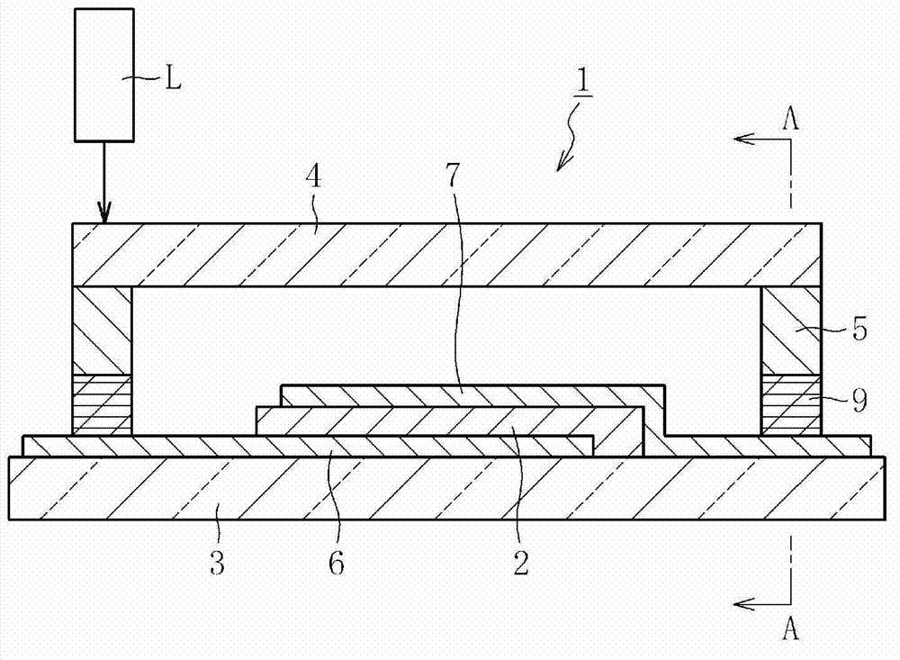
An organic electroluminescent(EL) device package 1 has an organic EL layer 2 hermetically sealed in an internal space, and includes a device substrate 3, a sealing substrate 4, a glass frit 5 and a protective film. The organic EL layer 2 is disposed on the device substrate 3. The sealing substrate 4 faces across an interval to a surface of the device substrate 3 at the side of the organic EL layer 2. The glass frit 5 hermetically seals the interval between the device substrate 3 and the sealing substrate 4 by surrounding the periphery of the organic EL layer 2. The protective film is disposed between the device substrate 3 and the glass frit 5, and is used to protect an electrode from the laser irradiated for melting the glass frit 5. Furthermore, the protective film, for example, is a dielectric multilayer film 8 which is effective as a reflective film for reflecting the laser, and the dielectric multilayer film 8 is formed by laminating a low refractivity dielectric layer and a high refractivity dielectric layer alternatively.

Description

technical field [0001] The present invention relates to an electrical component package that hermetically seals electrical components that are very sensitive to the surrounding environment, such as organic EL, in order to prevent deterioration due to oxygen and moisture in the surrounding environment. Background technique [0002] As is well known, organic EL display devices (organic EL displays) have been researched and developed in various ways, and have been put into practical use in some fields such as small display devices used in mobile phones and the like. [0003] The organic EL element (organic EL layer) used in this organic EL display device is a sensitive element that is easily degraded by exposure to oxygen and moisture in the surrounding environment. Therefore, at the time of practical use, by incorporating the organic EL layer into an organic EL display device in a hermetically sealed state, the display quality of the device can be maintained and the lifetime c...

Claims


Application Information

Patent Timeline
Patent Type & Authority Applications(China)
IPC IPC(8): H05B33/04C03C8/24H01L31/042H01L51/50
CPCC03C8/08H01L51/5246C03C8/24H05B33/04C03C3/19H01L2924/16195H10K59/8722B65D85/00H10K50/8426
Inventor 山崎康夫白神彻益田纪彰樱井武山崎博树
Owner NIPPON ELECTRIC GLASS CO LTD
Learn More