
A kind of Schottky diode and its preparation method

A Schottky diode and cathode technology, which is used in the manufacture of semiconductor/solid-state devices, electrical components, circuits, etc., can solve the limitation of reverse voltage withstand capability, complex process, and difficulty in withstand voltage and conduction capability of Schottky diodes and other problems, to achieve the effect of improving the conduction capacity and increasing the withstand voltage

Active Publication Date: 2015-11-25
SUZHOU YINGNENG ELECTRONICS TECH
View PDF3 Cites 0 Cited by
  • Summary
  • Abstract
  • Description
  • Claims
  • Application Information

AI Technical Summary

Problems solved by technology

[0006]First, in the Schottky diode disclosed in this document, the high barrier region 114 is recessed and formed on the top surface of the AlGaN layer. In the actual manufacturing process , the heterojunction of GaN and AlGaN needs to be formed by epitaxial growth first, and then a downwardly recessed opening needs to be defined on the top surface of the formed AlGaN to inject materials with higher band gap energy, thereby forming a high In the barrier region 114, in this process, due to the need to define openings in advance (generally by digging out a part of AlGaN), not only the process is complicated, but also after injecting materials with higher bandgap energy into the openings, it is easy to contact between the two. More defects are formed in the parts, which affects the improvement of the final withstand voltage capability of the Schottky diode, and thus limits the improvement of its reverse withstand voltage capability;
[0007]Second, in the Schottky diode disclosed in this document, the high potential barrier region is composed of AlGaN layer, and Mg, Cd are implanted in the AlGaN layer , Zn, Ca, N, O, C or a silicon dioxide layer to modify the AlGaN layer to form a high barrier region. In this process, the inventors only pay attention to planting Whether the implanted element layer helps to form a high-bandgap energy or a high-resistivity high barrier region, regardless of whether the implanted element helps to improve the forward conduction capability of the Schottky diode. In fact, according to the above It is recorded that when the implanted elements are N, O, C or even an inert gas, it cannot play a good role in improving the forward conduction capability of the Schottky diode, so that it is difficult for the Schottky diode disclosed in this document to simultaneously Ensure good withstand voltage and conduction capability, which in turn affects its application in the integration of power devices
Therefore, it is difficult for those skilled in the art to obtain the technical enlightenment of using the P-AlGaN layer to improve the forward conduction capability and reverse withstand voltage capability of Schottky diodes from this document
[0009] To sum up, there is a lack of a Schottky diode that can simultaneously improve forward conduction capability and reverse withstand voltage capability in the prior art

Method used


Image

  • A kind of Schottky diode and its preparation method
  • A kind of Schottky diode and its preparation method
  • A kind of Schottky diode and its preparation method

Examples


Embodiment 1

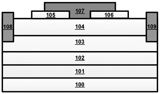
[0058] This embodiment provides a Schottky diode, including a substrate layer 100 formed of sapphire, a crystal nucleus layer 101 above the substrate layer, a buffer layer 102 above the crystal nucleus layer 101, and GaN formed on the buffer layer 102. layer 103 and the AlGaN layer 104 located on the GaN layer 103, a two-dimensional electron gas channel is formed between the GaN layer 103 and the AlGaN layer 104, and the GaN layer 103 and the AlGaN layer 104 form ohmic contacts with the cathodes 108 and 109, and the AlGaN layer 104 It forms a Schottky contact with the anode electrode; it also includes a metal field plate 107 connected to the anode electrode and annular P-GaN enhancement layers 105 and 106 filled between the metal field plate 107 and the AlGaN layer 104 .

[0059] In this embodiment, the doping concentration of the two P-GaN enhancement layers 105, 106 is between 1E13-1E20 / cm 3 In between, the doping concentration increases gradually along the direction extendi...

Embodiment 2

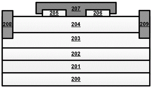
[0069]This embodiment provides a Schottky diode, including a substrate layer 200 formed of Si, a crystal nucleus layer 201 located above the substrate layer, a buffer layer 202 located above the crystal nucleus layer 201, and a GaN layer formed on the buffer layer 202. layer 203 and the AlGaN layer 204 located on the GaN layer 203, a two-dimensional electron gas channel is formed between the GaN layer 203 and the AlGaN layer 204, and the GaN layer 203 and the AlGaN layer 204 form ohmic contacts with the cathodes 208 and 209, and the AlGaN layer 204 It forms a Schottky contact with the anode electrode; it also includes a metal field plate 207 connected to the anode electrode and annular P-GaN enhancement layers 205 and 206 filled between the metal field plate 207 and the AlGaN layer 204 .

[0070] In this embodiment, the doping concentration of the two P-GaN enhancement layers 205, 206 is between 1E13-1E20 / cm 3 In between, the doping concentration increases gradually along the ...

Embodiment 3

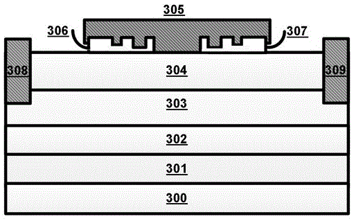
[0080] This embodiment provides a Schottky diode, including a substrate layer 300 formed of SiC, a crystal nucleus layer 301 located above the substrate layer, a buffer layer 302 located above the crystal nucleus layer 301, and a GaN layer formed on the buffer layer 302. layer 303 and the AlGaN layer 304 located on the GaN layer 303, a two-dimensional electron gas channel is formed between the GaN layer 303 and the AlGaN layer 304, the GaN layer 303 and the AlGaN layer 304 form ohmic contacts with the cathodes 308, 309, and the AlGaN layer 104 It forms a Schottky contact with the anode electrode; it also includes a metal field plate 305 connected to the anode electrode and annular P-GaN enhancement layers 307 and 307 filled between the metal field plate 305 and the AlGaN layer 304 .

[0081] In this embodiment, the doping concentration of the P-GaN enhancement layers 307, 306 is between 1E13-1E20 / cm 3 Between, more specifically, the doping concentrations of the different regio...


PUM


Abstract

The invention provides a Schottky diode which comprises a substrate layer as well as a series of III-family nitride layers formed above the substrate layer, a metal field plate connected with the anode electrode and at least one P-type doped III-family nitride reinforcement layer which is filled between the metal field plate and a III-family nitride layer at the uppermost layer. Two-dimensional electron gas channels are formed between the adjacent III-family nitride layers by utilizing a heterogeneous structure; the III-family nitride layers and a cathode electrode are in ohmic contact; and the III-family nitride layers and an anode electrode are in Schottky contact. According to the Schottky diode provided by the inventio, the reverse withstand voltage capability and the forward withstand voltage capability are improved at the same time.

Description

technical field [0001] The invention relates to a Schottky diode and a preparation method thereof, belonging to the technical field of semiconductors. Background technique [0002] Diodes are widely used in power circuits. The ideal diode expected by a typical power circuit should include the following characteristics: First, when the device is in a reverse bias state (the cathode voltage is much higher than the anode voltage), the diode needs to be able to bear as much as possible High voltage, its withstand voltage depends on the performance requirements of the circuit for the device. In many high-voltage power switching applications, the diode is required to bear the back voltage of 600V or 1200V; second, when the device is in the forward biased state, it needs its The forward conduction voltage should be as low as possible to reduce the conduction loss, that is, a sufficiently low forward conduction resistance is required; third, the charge stored in the diode should be ...

Claims


Application Information

Patent Timeline
Patent Type & Authority Patents(China)
IPC IPC(8): H01L29/872H01L29/06H01L21/329
Inventor 谢刚汤岑盛况郭清汪涛崔京京
Owner SUZHOU YINGNENG ELECTRONICS TECH
Learn More