Patterned multilayer array paper chip, preparation method and application thereof

A multi-layer array, paper chip technology, applied in chemical instruments and methods, analysis by chemical reaction of materials, containers for laboratory use, etc. The effect of fast kinetic process, low cost and simple operation

Inactive Publication Date: 2013-02-06
DALIAN UNIV
View PDF3 Cites 54 Cited by
  • Summary
  • Abstract
  • Description
  • Claims
  • Application Information

AI Technical Summary

Problems solved by technology

[0005] Another object of the present invention is to provide a preparation method for the above-mentioned chip, so

Method used


Image

  • Patterned multilayer array paper chip, preparation method and application thereof
  • Patterned multilayer array paper chip, preparation method and application thereof
  • Patterned multilayer array paper chip, preparation method and application thereof

Examples


Embodiment 1

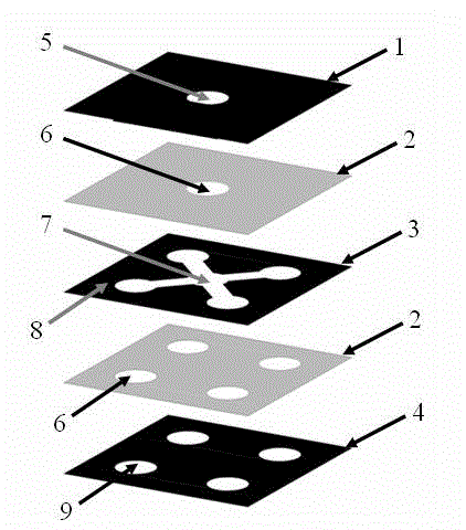
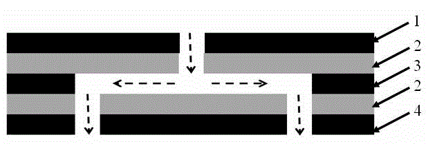
[0019] Put Whatman? No. 1 filter paper into the wax jet printer, and print the designed pattern on the filter paper (such as image 3 shown), and press the image 3 Cut out the outer contour; bake the cut filter paper in an oven at 140°C for 3 minutes; take out the baked filter paper and place it in a dark place until its temperature drops to room temperature. Put 3M-300lse double-sided tape, press image 3 The pattern shown is punched and contoured. Peel off the protective film on one side of the double-sided tape, stick it to the first filter paper layer, then peel off the other protective film, and stick it to the second filter paper layer. Repeat the above steps until the assembly of the entire patterned multilayer array paper chip is completed. The schematic diagram of the structure of the multilayer array paper chip prepared according to the above steps is as follows: image 3 shown. Through this chip, a single sample can be divided into 16 parallel samples in paral...

Embodiment 2

[0021] Put Whatman? No. 1 filter paper into the wax jet printer, and print the designed pattern on the filter paper (such as Figure 4 shown), and press the Figure 4 Cut out the outer contour; bake the cut filter paper in an oven at 140°C for 3 minutes; take out the baked filter paper and place it in a dark place until its temperature drops to room temperature. Put 3M-300lse double-sided tape, press Figure 4 The pattern shown is punched and contoured. Peel off the protective film on one side of the double-sided tape, stick it to the first filter paper layer, then peel off the other protective film, and stick it to the second filter paper layer. Repeat the above steps until the assembly of the entire patterned multilayer array paper chip is completed. The schematic diagram of the structure of the multilayer array paper chip prepared according to the above steps is as follows: Figure 4 shown. Through this chip, the 4 samples to be tested can be divided into 4 parallel sa...

Embodiment 3

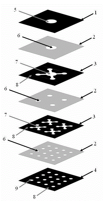
[0023] Put Whatman? No. 1 filter paper into the wax jet printer, and print the designed pattern on the filter paper (such as Figure 5 shown), and press the Figure 5 Cut out the outer contour; bake the cut filter paper in an oven at 140°C for 3 minutes; take out the baked filter paper and place it in a dark place until its temperature drops to room temperature. Put 3M-300lse double-sided tape, press Figure 5 The pattern shown is punched and contoured. Peel off the protective film on one side of the double-sided tape, stick it to the first filter paper layer, then peel off the other protective film, and stick it to the second filter paper layer. Repeat the above steps until the assembly of the entire patterned multilayer array paper chip is completed. The schematic diagram of the structure of the multilayer array paper chip prepared according to the above steps is as follows: Figure 5 shown. Through this chip, each of the 4 samples to be tested can be divided into 4 par...


PUM


Abstract

The invention provides a patterned multilayer array paper chip, a preparation method and an application thereof. The front surface, rear surface and interior of the patterned multilayer array paper chip all have the structures of alternately emerged wax areas and filter paper areas and alternately emerged hydrophilic areas and lyophobic areas. The preparation method comprises the following steps: designing a required pattern by using a computer; printing the wax onto an untreated filter paper surface by using a printing machine; placing a printed patterned multilayer array paper chip into a high-temperature container for roasting; and then taking out and cooling; and packaging, thereby obtaining the wax patterned multilayer array paper chip. The patterned multilayer array paper chip is applied to the high-flux and quick detection for environmental pollutants, such as, the assay determination for heavy metal ions in suitably treated agricultural products, such as, vegetables, neutralized by water. The preparation method provided by the invention is simple, direct, low-cost, high in preparing speed, suitable for mass production of the patterned multilayer array paper chip, and has commercial prospect.

Description

technical field [0001] The invention relates to related research in the fields of microfluidic chip technology and environmental pollutant analysis and detection, and in particular provides a patterned multilayer array paper chip, a preparation method and an application thereof. Background technique [0002] The chip is the foundation and key of microfluidic chip research, and the material and design of the chip determine its endowed functions. The materials used in common microfluidic chips include silicon, quartz, glass and organic polymers such as polymethyl methacrylate (PMMA), polydimethylsiloxane (PDMS), etc. With the continuous development of chip research, the material of the chip is gradually expanding. In early 2007, the Whitesides group of Harvard University first tried to use paper as a material for the production of microfluidic chips. Paper materials have some special advantages such as: (1) Low cost: suitable for preparing disposable chips; (2) The cellulose ...

Claims


Application Information

Patent Timeline
IPC IPC(8): G01N21/78B01L3/00
Inventor 郑国侠李雅杰王云华魏俊峰
Owner DALIAN UNIV
Why Eureka
Try Eureka