Preparation method of silylene material

A silicene and semiconductor technology, applied in the field of nanomaterials, can solve problems such as the inability to separate silicene by tape stripping

Active Publication Date: 2013-02-13
INST OF PHYSICS - CHINESE ACAD OF SCI
View PDF2 Cites 9 Cited by
  • Summary
  • Abstract
  • Description
  • Claims
  • Application Information

AI Technical Summary

Problems solved by technology

However, there is no layered structure in the bulk material of sili

Method used


Image

  • Preparation method of silylene material
  • Preparation method of silylene material
  • Preparation method of silylene material

Examples


Embodiment Construction

[0024] The preparation method of silylene will be further described in detail below in conjunction with the drawings and embodiments. This embodiment is only used for more detailed description, and should not be construed as limiting the present invention in any form.

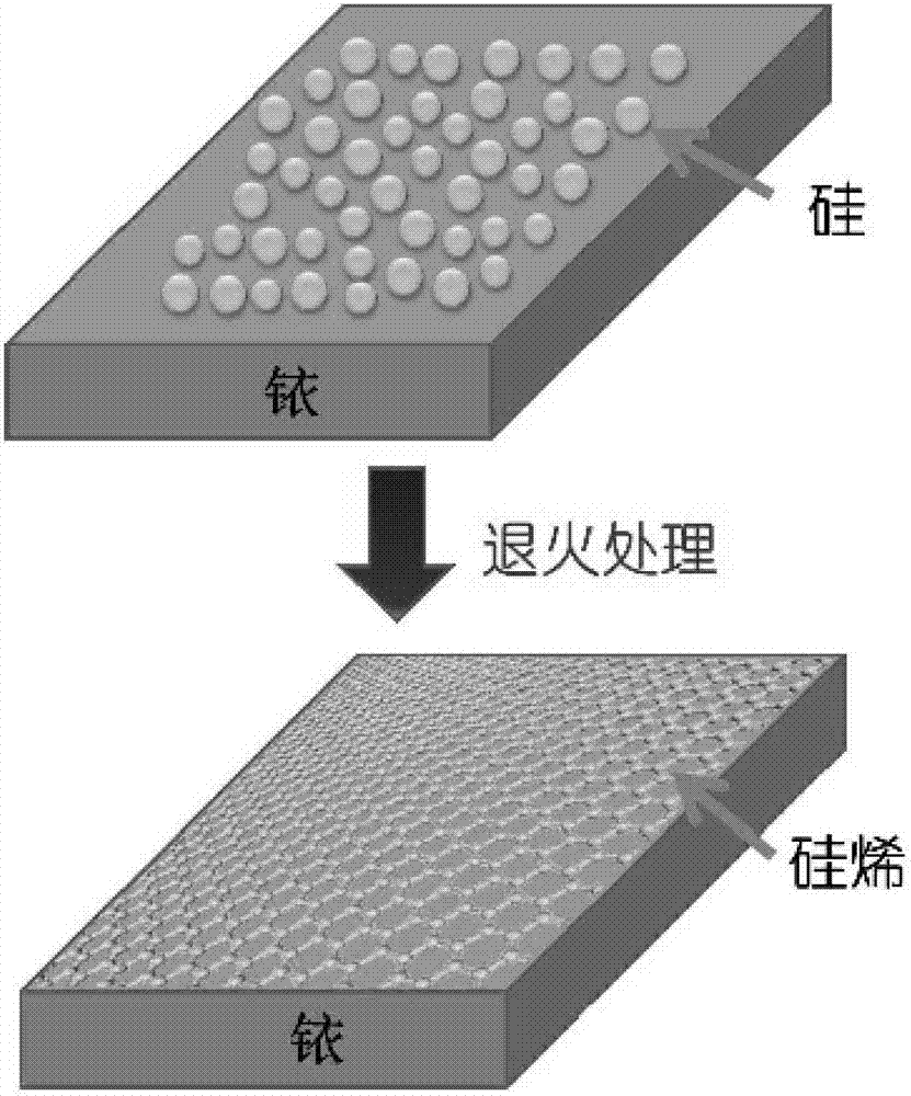
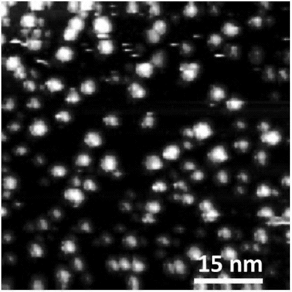
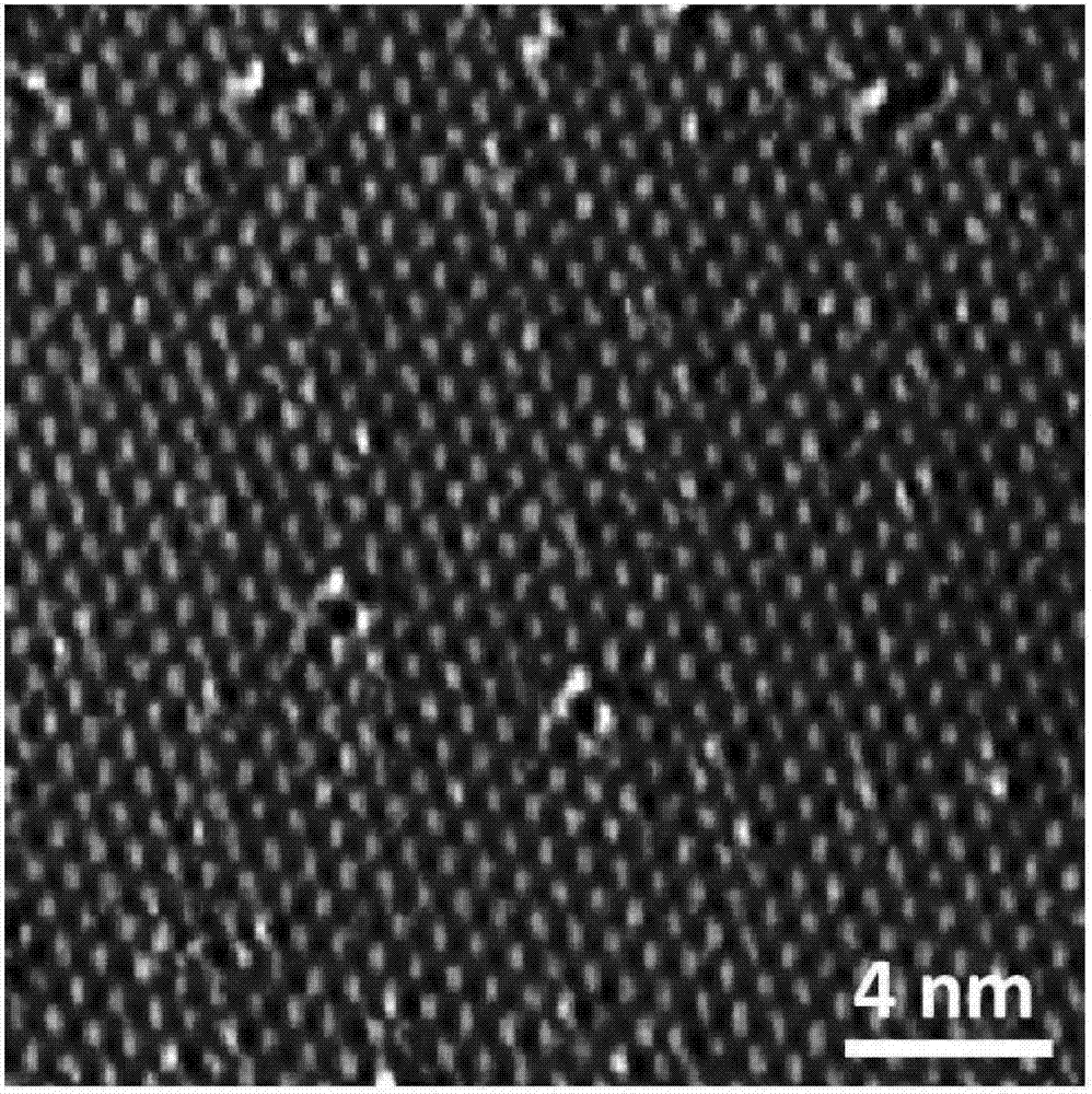
[0025] In this embodiment, high-quality silylene is prepared on the surface of the transition metal. The specific steps are as follows: firstly, the iridium single crystal is sputtered with argon ion several times or more than ten times in the vacuum chamber, and then the iridium substrate is heated and maintained at 850° C., and high temperature annealing is performed to obtain a clean and flat (111) crystal plane. The effect schematic diagram of the overall preparation process of the present invention is as follows figure 1 Shown. The upper part of the figure shows the high-coverage silicon particles deposited on the (111) surface of iridium in the present invention; the lower part of the figure shows the two-d...


PUM


Abstract

The invention discloses a preparation method of a silylene material. The preparation method comprises the following steps of 1) evaporating and depositing a proper amount of silicons to a transitional metal iridium substrate; and 2) annealing the whole sample so that the silicons are interacted with each other; forming a two-dimensional orderly film-shaped structure on the surface of the substrate; and arranging silicon atoms in a hexagonal honeycomb shape, so as to form a novel two-dimensional crystal material-silylene. The novel material is similar to graphene and obtains wide application potential in the future development and research aspect of information electronics and devices.

Description

Technical field [0001] The invention relates to a method for preparing a silylene material and belongs to the technical field of nano materials. Background technique [0002] New two-dimensional crystal materials have become the focus of research in recent years because of their single-atom thickness two-dimensional crystal structure and unique physical properties. When microelectronics is gradually entering the limit of physical size and facing a development bottleneck, the development and application of new two-dimensional crystal materials represented by graphene are expected to break through the bottleneck problems encountered by large-scale integrated circuits at present, which is the foundation of our country Research fields such as science, information science, material science, and energy science provide a new opportunity and platform, and have a profound impact on the sustainable development of the national economy and national defense security. For example, graphene ex...

Claims


Application Information

Patent Timeline
IPC IPC(8): C01B33/04
Inventor 王业亮孟蕾高鸿钧
Owner INST OF PHYSICS - CHINESE ACAD OF SCI
Why Eureka
Try Eureka