Packaging element of semiconductor device
A package and semiconductor technology, which is applied in the direction of semiconductor devices, semiconductor/solid-state device components, electric solid-state devices, etc. rate, the effect of increasing the contact area
- Summary
- Abstract
- Description
- Claims
- Application Information
AI Technical Summary
Problems solved by technology
Method used
Image

Examples
no. 1 example
[0033] Please refer to Figure 4 , the semiconductor device packaging method of the first embodiment of the present invention, comprising:
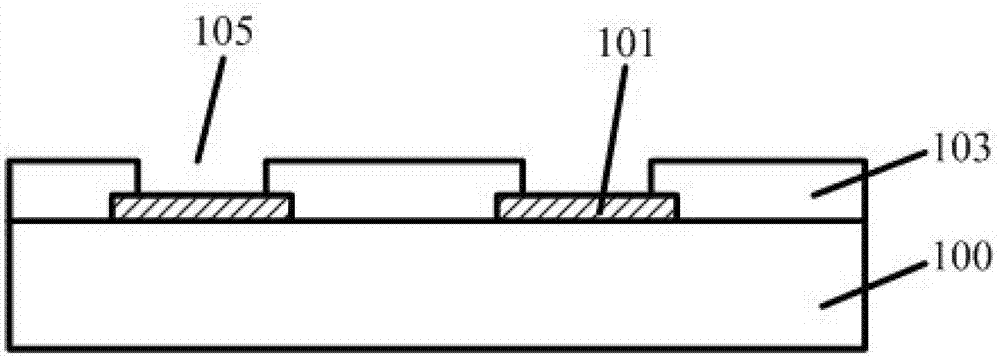
[0034] Step S201, providing a chip with a pad on its surface, a passivation layer is formed on the surface of the chip, and the passivation layer has an opening exposing part of the pad surface;
[0035] Step S202, forming a bump on the surface of the pad in the opening, the size of the bump is smaller than the size of the opening;
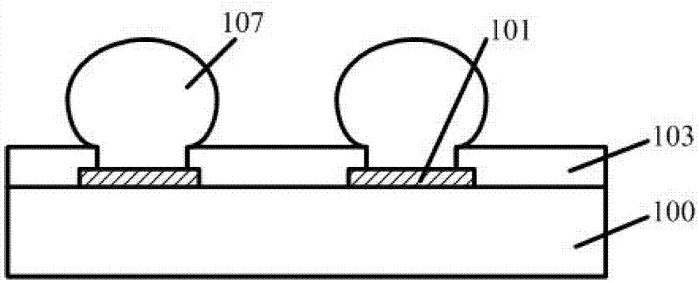
[0036] Step S203 , forming a solder ball covering the surface of the bump and covering the surface of the pad at the bottom of the opening.
[0037] Specifically, please refer to Figure 5-Figure 8 , Figure 5-Figure 8 A schematic cross-sectional structure showing the packaging process of the semiconductor device according to the first embodiment of the present invention.
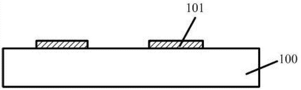
[0038] Please refer to Figure 5 , provide a chip 300 with pads 301 on its surface, a passivation layer 303 is formed on the surface...
no. 2 example
[0060] Different from the first embodiment of the present invention, in the second embodiment of the present invention, an anti-diffusion layer is formed on the top surface and side surface of the bump to prevent copper atoms in the bump and solder balls from The interdiffusion of tin atoms affects the bonding strength of solder balls. Moreover, the surface of the anti-diffusion layer is also covered with a wetting layer to improve the bonding force between the anti-diffusion layer and the solder balls.
[0061] Please refer to Figure 8 , in the second embodiment of the present invention, the packaging method of the semiconductor device includes:
[0062] Step S401, providing a chip with a pad on its surface, a passivation layer is formed on the surface of the chip, and the passivation layer has an opening exposing part of the pad surface;
[0063] Step S402, forming a bump on the surface of the pad in the opening, the size of the bump is smaller than the size of the openin...
no. 3 example
[0091] Slightly different from the second embodiment of the present invention, the anti-diffusion layer not only covers the surface of the bump, but also covers the surface of the pad in the opening, forming a skirt structure, so that the solder ball can more easily cover the surface of the pad when forming a solder ball , to further increase the strength of the solder ball.
[0092] Please refer to Figure 13 , the semiconductor device packaging method of the third embodiment of the present invention, comprising:
[0093] Step S601, providing a chip with a pad on its surface, a passivation layer is formed on the surface of the chip, and the passivation layer has an opening exposing part of the pad surface;
[0094] Step S602, forming a bump on the surface of the pad in the opening, the size of the bump is smaller than the size of the opening;
[0095] Step S603, forming an anti-diffusion layer covering the surface of the bump and covering the surface of the pad at the botto...
PUM
 Abstract
Description
Claims
Application Information
 - R&D
- Intellectual Property
- Life Sciences
- Materials
- Tech Scout
- Unparalleled Data Quality
- Higher Quality Content
- 60% Fewer Hallucinations
Browse by: Latest US Patents, China's latest patents, Technical Efficacy Thesaurus, Application Domain, Technology Topic, Popular Technical Reports.
© 2025 PatSnap. All rights reserved.Legal|Privacy policy|Modern Slavery Act Transparency Statement|Sitemap|About US| Contact US: help@patsnap.com