N-channel metal oxide semiconductor (NMOS) transistor and forming method thereof

A technology of transistors and semiconductors, applied in semiconductor devices, semiconductor/solid-state device manufacturing, electrical components, etc., can solve the problems of limited performance improvement of transistors, small improvement of carrier mobility, limited stress, etc., and achieve the goal of improving mobility Effect

Active Publication Date: 2013-02-13
SEMICON MFG INT (SHANGHAI) CORP
View PDF13 Cites 4 Cited by
  • Summary
  • Abstract
  • Description
  • Claims
  • Application Information

AI Technical Summary

Problems solved by technology

[0005] However, in the prior art, the source / drain region of the transistor is a rectangular structure, the stress on the channel region under the gate structure is limited, the improvement of the carrier mobility is small, and the performance of the transistor is limited. Therefore, the industry needs MOS devices capable of greater stress

Method used


Image

  • N-channel metal oxide semiconductor (NMOS) transistor and forming method thereof
  • N-channel metal oxide semiconductor (NMOS) transistor and forming method thereof
  • N-channel metal oxide semiconductor (NMOS) transistor and forming method thereof

Examples


no. 1 example

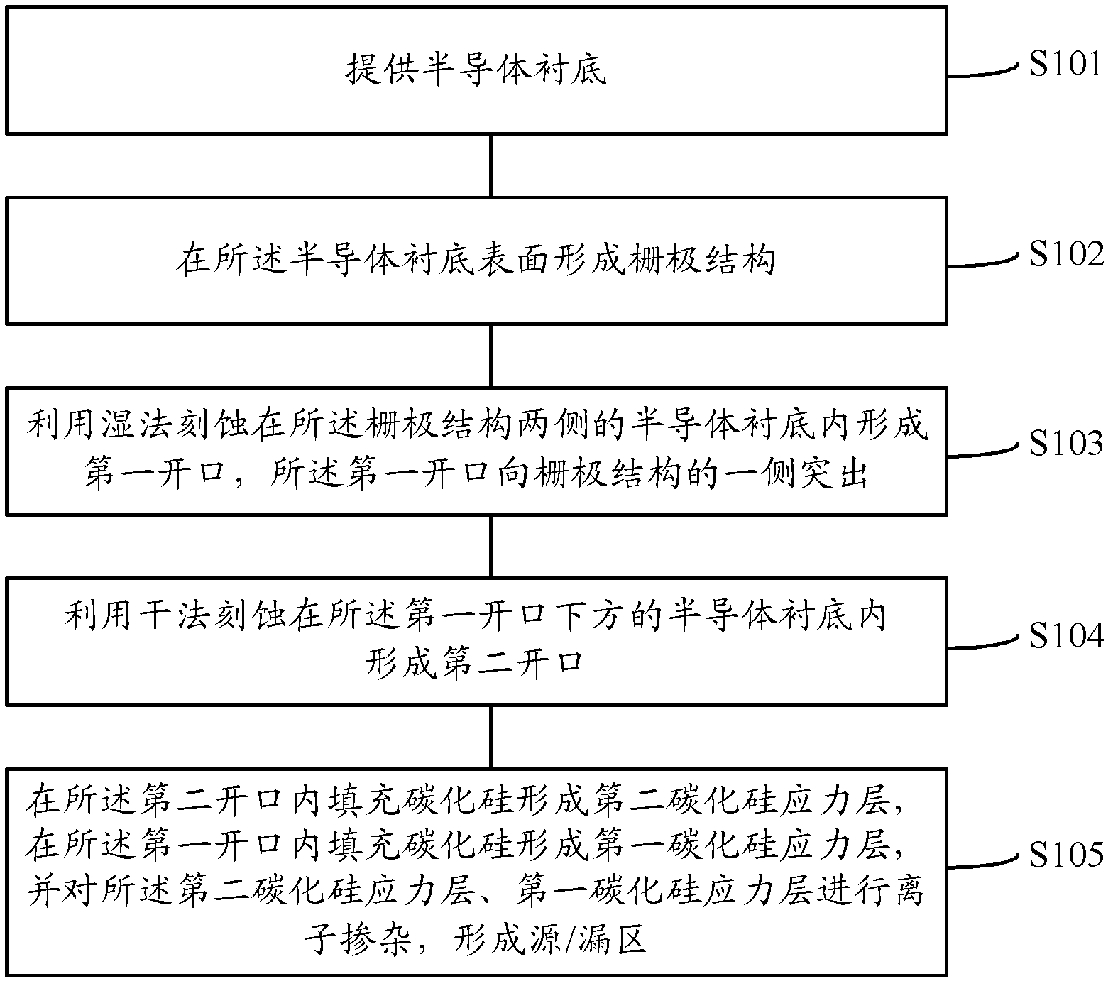
[0056] Please refer to figure 2 , is a schematic flowchart of the method for forming an NMOS transistor according to the first embodiment of the present invention, specifically including:

[0057] Step S101, providing a semiconductor substrate;

[0058] Step S102, forming a gate structure on the surface of the semiconductor substrate;

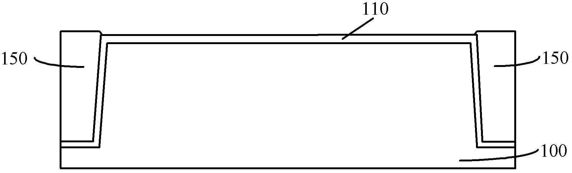
[0059] Step S103, using wet etching to form first openings in the semiconductor substrate on both sides of the gate structure, and the first openings protrude toward one side of the gate structure;

[0060] Step S104, forming a second opening in the semiconductor substrate below the first opening by dry etching;

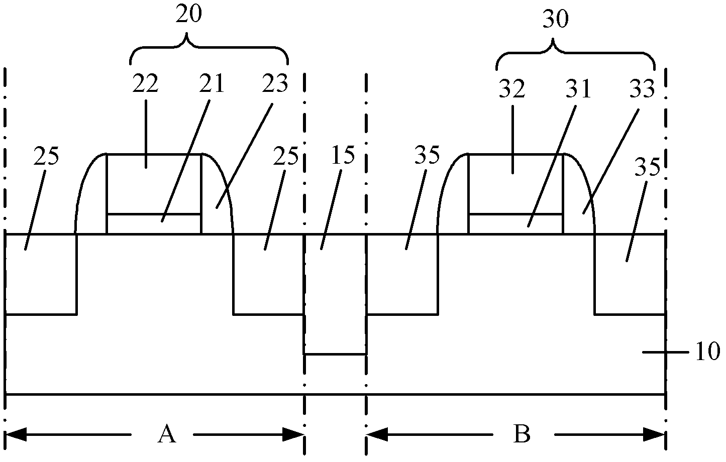
[0061] Step S105, filling the second opening with silicon carbide to form a second silicon carbide stress layer, filling the first opening with silicon carbide to form a first silicon carbide stress layer, and adding the second silicon carbide stress layer, Ion doping is performed on the first silicon carbide stress layer to form ...

no. 2 example

[0099] Please refer to Figure 11 , is a schematic flow chart of the method for forming an NMOS transistor according to the second embodiment of the present invention, specifically including:

[0100] Step S201, providing a semiconductor substrate;

[0101] Step S202, forming a gate structure on the surface of the semiconductor substrate;

[0102] Step S203, using wet etching to form first openings in the semiconductor substrate on both sides of the gate structure, the first openings protruding to one side of the gate structure;

[0103] Step S204, performing carbon ion doping on the semiconductor substrate below the first opening to form a second silicon carbide stress layer;

[0104] Step S205 , filling the first opening with silicon carbide to form a first silicon carbide stress layer, and performing ion doping on the second silicon carbide stress layer and the first silicon carbide stress layer to form source / drain regions.

[0105] Figure 12 to Figure 14 It is a sche...


PUM

PropertyMeasurementUnit
Depth rangeaaaaaaaaaa
Thicknessaaaaaaaaaa
Thickness rangeaaaaaaaaaa

Abstract

The invention relates to an N-channel metal oxide semiconductor (NMOS) transistor and a forming method thereof. The NMOS transistor comprises a semiconductor substrate, a gate structure and source / drain regions, wherein the gate structure is positioned on the surface of the semiconductor substrate; the source / drain regions are positioned in the semiconductor substrate on the two sides of the gate structure and comprise first silicon carbide stress layers positioned in the semiconductor substrate on the two sides of the gate structure, and second silicon carbide stress layers which are positioned at the bottoms of the first silicon carbide stress layers and in contact with the first silicon carbide stress layers; and the first silicon carbide stress layers protrude out of one side of the gate structure. The first silicon carbide stress layers protrude out of one side of the gate structure, and the depth of the second silicon carbide stress layers is large, so that tensile stress generated by the source / drain regions of the NMOS transistor is high, the lattice spacing of a channel region of the NMOS transistor is large, and electron mobility is high.

Description

technical field [0001] The invention relates to semiconductor manufacturing technology, and more specifically, the invention relates to an NMOS transistor capable of improving carrier mobility and a forming method thereof. Background technique [0002] It is well known that stress can change the energy gap and carrier mobility of silicon materials. With the in-depth research on the piezoresistance effect of silicon materials, the industry has gradually realized that stress can be used to increase the carrier mobility of MOS devices, that is, strained silicon technology (Strained Silicon). [0003] The U.S. patent document with publication number US2007 / 0196992A1 discloses a strained silicon CMOS transistor with silicon germanium and silicon carbide source / drain regions, please refer to figure 1 , including: a semiconductor substrate 10, the semiconductor substrate 10 includes a region A where an NMOS transistor is to be formed and a region B where a PMOS transistor is to be...

Claims


Application Information

Patent Timeline
IPC IPC(8): H01L29/78H01L29/06H01L21/336
Inventor 赵猛三重野文健
Owner SEMICON MFG INT (SHANGHAI) CORP
Why Eureka
Try Eureka