Thin-film photovoltaic devices using enhanced light-harvesting schemes

A device and light absorption technology, applied in photovoltaic power generation, semiconductor devices, electrical components, etc., to achieve the effect of saving deposition time

Inactive Publication Date: 2015-08-05
DSM IP ASSETS BV
View PDF9 Cites 0 Cited by
  • Summary
  • Abstract
  • Description
  • Claims
  • Application Information

AI Technical Summary

Problems solved by technology

This texturing method also has the disadvantages already discussed

Method used


Image

  • Thin-film photovoltaic devices using enhanced light-harvesting schemes
  • Thin-film photovoltaic devices using enhanced light-harvesting schemes
  • Thin-film photovoltaic devices using enhanced light-harvesting schemes

Examples


example 1

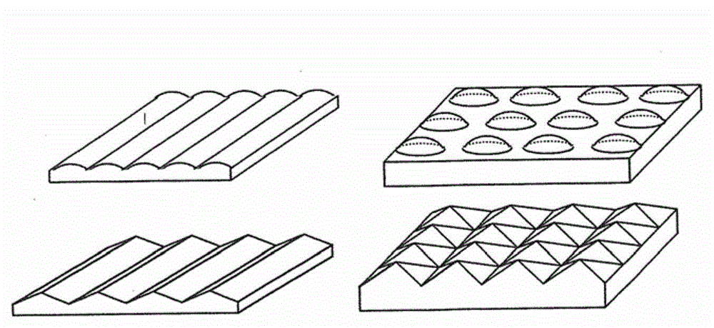
[0040] produces a polymer plate, which includes such as Figure 4 An array of structures as described in . Thin-film silicon modules based on a tandem junction cell structure with two light-absorbing active layers and an upper cell consisting of amorphous silicon and a bottom cell consisting of microcrystalline silicon were fabricated. The TCO in the module is based on a non-textured 50nm thick aluminum-doped zinc oxide layer. Silver was used as the reflective back electrode. The polymer sheet was applied to the glass front cladding of the thin film silicon module by lamination with a sheet of EVA.

example 2

[0042] produce polymer sheets, which include such as Figure 4 An array of structures as described in . Thin-film silicon modules based on a tandem junction cell structure with two light-absorbing active layers and an upper cell consisting of amorphous silicon and a bottom cell consisting of microcrystalline silicon were fabricated. The TCO in the module is based on a non-textured 50nm thick aluminum-doped zinc oxide layer. Silver was used as the reflective back electrode. The polymer sheet is applied to the glass front cladding of the thin-film silicon module by a silicone-based adhesive.

example 3

[0044] produces a polymer plate, which includes such as Figure 4 An array of structures as described in . Fabrication of thin-film silicon modules based on -Si / μc-Si based photovoltaic modules including textured superstrate, non-textured 100-400nm ZnO, 150-200nm a-Si i-layer, 500-800nm ​​μc -Si i-layer. Silver was used as the reflective back electrode. The polymer plate is applied to the glass front cladding of the thin film silicon module by using a polymer adhesive.
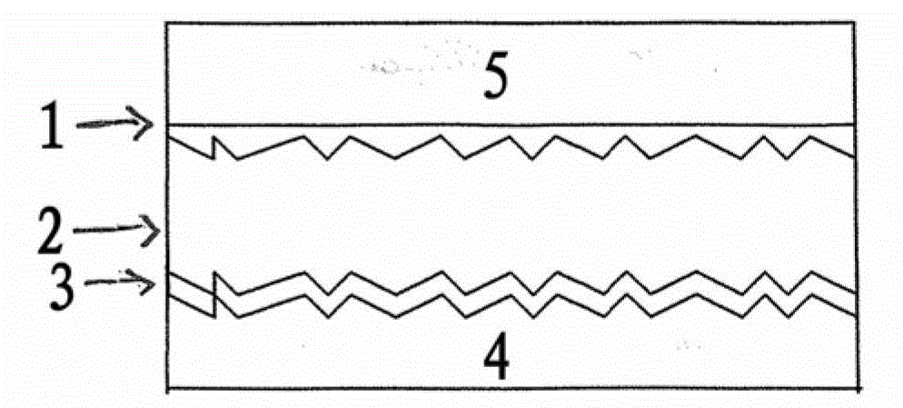
[0045] figure 1 :

[0046] figure 1 Methods of reducing the layer thickness of the active material or active layer 2 according to the prior art are shown. The purpose of this is to create a texture of refracted light in the front electrode or TCO1. As a result of the refraction of light, the path length of light entering the active material 2 increases. However, the control of the refraction of light is limited and thus the increase in path length is small. Also, texturing introduces defects in TCO1 t...


PUM


Abstract

A thin film photovoltaic device comprising a relief textured transparent cover plate, a layer of transparent conductive oxide having a layer thickness of less than 700 nm, a light absorbing active layer and a reflective back electrode, where the layer of transparent conductive oxide is a non-textured layer.

Description

technical field [0001] The present invention relates to a thin film photovoltaic device comprising a relief textured transparent superstrate, a transparent conductive oxide layer (TCO), a light absorbing active layer and a reflective back electrode. Background technique [0002] Photovoltaic devices are generally used to convert light energy into electrical energy. These devices contain active layers with light absorbing materials that generate charge carriers upon exposure to light. Typical examples of such materials are monocrystalline silicon (m-Si) and polycrystalline silicon (p-Si). Because silicon is expensive, it is important to keep the layer thickness to a minimum. In the case of m-Si and p-Si, the layer thicknesses are relatively thick, since this material is also used as a substrate for the manufacture of photovoltaic devices. The overall layer thickness of silicon is therefore approximately 180 μm. To overcome this and other problems, thin film photovoltaic d...

Claims


Application Information

Patent Timeline
Patent Type & Authority Patents(China)
IPC IPC(8): H01L31/0236H01L31/048
CPCY02E10/50H01L31/046H01L31/0236H01L31/048
Inventor K·赫尔曼斯B·斯拉格尔B·C·克兰兹A·霍夫曼
Owner DSM IP ASSETS BV
Why Eureka
Try Eureka