Post-CMOS integrated method for threshold presetting

A MOS tube and threshold technology, applied in gaseous chemical plating, process for producing decorative surface effects, coating, etc., can solve problems such as inability to obtain input results, asymmetric threshold of MOS tube, etc., and reduce process complexity , high yield, reducing the effect of parasitic capacitance and distributed capacitance

Inactive Publication Date: 2013-02-20
PEKING UNIV
View PDF5 Cites 4 Cited by
  • Summary
  • Abstract
  • Description
  • Claims
  • Application Information

AI Technical Summary

Problems solved by technology

This kind of situation is very easy to happen in the part of the operational amplifier. The threshold value of the MOS transistor at the positive and negative input terminals is asymmetrical, which makes it impossible to get the correct input result.

Method used


Image

  • Post-CMOS integrated method for threshold presetting
  • Post-CMOS integrated method for threshold presetting
  • Post-CMOS integrated method for threshold presetting

Examples


Embodiment Construction

[0034] The present invention will be described in detail below through specific embodiments and accompanying drawings.

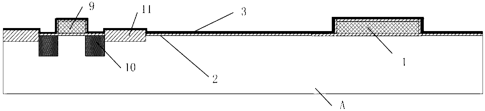
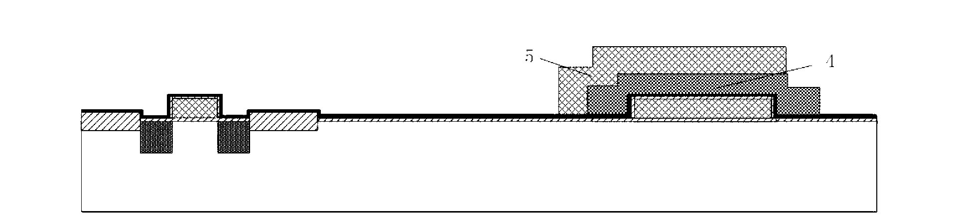
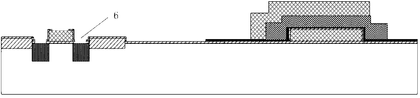
[0035] The integration method of the preset threshold value of the present invention is mainly applicable to MEMS device chips made on silicon substrates, including IC parts and movable structures realized by sacrificial layer technology, such as accelerometers, gyroscopes and other sensors, adjustable capacitors structure and other actuators. The following takes the preparation of a monolithic integrated planar capacitive resonator as an example to illustrate.

[0036] First estimate the stress that the MEMS process will introduce.

[0037] When estimating the amount of threshold drift caused by stress, those skilled in the art can obtain the stress value through simulation according to the materials and processes selected by MEMS, and then find other literature on the influence of stress in the field of microelectronic IC devices, and compare the numerica...


PUM

PropertyMeasurementUnit
thicknessaaaaaaaaaa

Abstract

The present invention provides a post-CMOS integrated method for threshold presetting. According to the method, a threshold drift magnitude introduced by a MEMS pre-estimating process is adopted to adjust a doping concentration of a CMOS process in an IC process to increase threshold symmetry of a MOS transistor after the post-CMOS process. According to the method, threshold drift defect is subjected to conversion utilization, special low-stress material production equipment is not required, MEMS movable structure and IC monolithic integration requirements can be met, and threshold symmetry of the MOS transistor of the integrated circuit portion can be ensured.

Description

technical field [0001] The invention belongs to the field of micro-electro-mechanical systems (MEMS) and integrated circuit IC (CMOS) processing technology, and relates to a monolithic integration method of MEMS and IC technology, and adopts a MEMS-IC-MEMS mixed technology method to simultaneously form MEMS and IC on a single wafer. The CMOS part is especially used in the field of manufacturing MEMS chips containing CMOS circuits. Background technique [0002] There are many advantages of monolithic integration of MEMS and IC, including reducing parasitic capacitance, reducing chip size, reducing cost, reducing packaging pressure, and improving reliability. The usually selected integration scheme is made by MEMS process after IC, that is, post-CMOS process. The design of post-CMOS integration scheme focuses on how to control the influence of MEMS process on IC circuit. Since IC circuits are composed of single-transistor NMOS or PMOS, studies have shown that the performance...

Claims


Application Information

Patent Timeline
Patent Type & Authority Applications(China)
IPC IPC(8): B81C1/00
Inventor 赵丹淇张大成何军黄贤杨芳田大宇刘鹏王玮李婷罗葵
Owner PEKING UNIV
Why Eureka
Try Eureka