Manufacturing method and device for reducing collector resistance through germanium-silicon HBT (Heterojunction Bipolar Transistor) with spuriously buried layer
A collector resistance and manufacturing method technology, applied in the manufacturing of electrical components, semiconductor devices, semiconductor/solid-state devices, etc., can solve problems such as performance affecting the cut-off frequency of radio frequency circuits, large contact resistance, etc., achieve proper location, and improve breakdown. voltage, the effect of increasing the output power gain
- Summary
- Abstract
- Description
- Claims
- Application Information
AI Technical Summary
Problems solved by technology
Method used
Image

Examples
Embodiment Construction
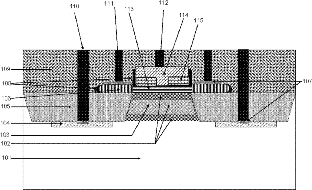
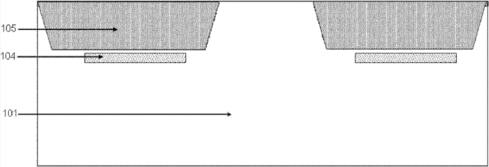
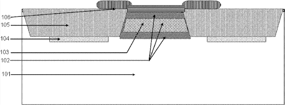
[0036] Such as figure 1 As shown, the silicon germanium HBT with the pseudo-buried layer in the embodiment of the present invention reduces the collector resistance of the device, and the active region is composed of shallow groove field oxygen, that is, figure 1 The shallow trench isolation layer 105 in isolation includes a collector region, a pseudo-buried layer, a base region and an emitter region.
[0037] A collector region is composed of a first ion implantation region 102 formed between the shallow trench isolation layer 105 and a second ion implantation region 103 formed at the edge of the active region and the shallow trench isolation layer 105, the first Both the ion implantation region 102 and the second ion implantation region 103 are N-type. The first ion implantation and the second ion implantation process together form a high-speed device, the implantation dose of the first ion implantation region 102 is relatively high, and the energy is low; the second ion im...
PUM
 Abstract
Description
Claims
Application Information