Preparation method for semiconductor device

A semiconductor and device technology, applied in the field of semiconductor device preparation, can solve the problems of long corrosion time, low yield, perforation and fracture of battery sheets, etc., and achieve the effects of reducing production cost, shortening length, improving stripping yield and production efficiency

Active Publication Date: 2013-03-06
DR TECH CO LTD YIXING JIANGSU
View PDF4 Cites 12 Cited by
  • Summary
  • Abstract
  • Description
  • Claims
  • Application Information

AI Technical Summary

Problems solved by technology

If the corrosion time is too long, the corrosion solution may penetrate the battery functional layer material from the defect of the battery functional layer material, causing the battery sheet to be perforated and broken, resulting in a low yield

Method used


Image

  • Preparation method for semiconductor device
  • Preparation method for semiconductor device
  • Preparation method for semiconductor device

Examples


Embodiment 1

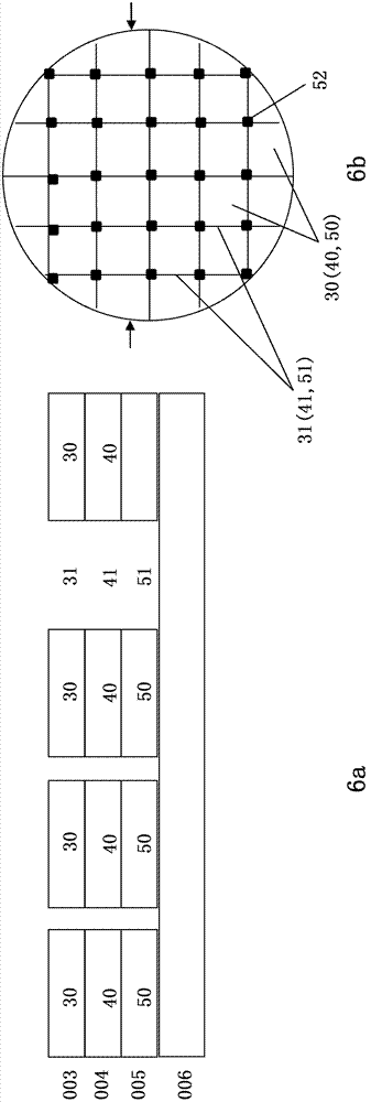
[0066] Refer to the attached figure 1 -8 Take gallium arsenide thin-film battery as an example to illustrate the process of preparing semiconductor devices of the present invention. Note that the drawings and the description of specific embodiments are only for better understanding of the present invention, and the present invention is not limited to the described embodiments.

[0067] The preparation process of the gallium arsenide thin film battery according to embodiment 1 is roughly as follows:

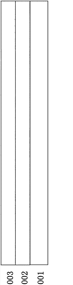
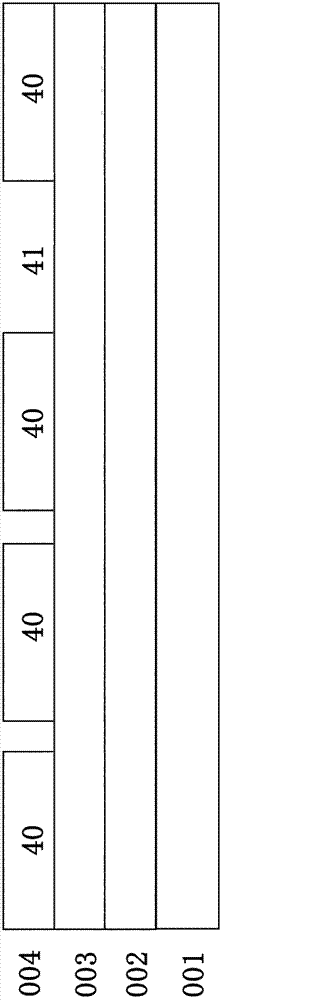
[0068] Step 1, preparing a battery functional layer on a gallium arsenide substrate, including:

[0069] Such as figure 1 As shown, prepare a gallium arsenide (GaAs) single crystal substrate 001 with a diameter of about 4 inches (10 cm) or more, and pass MOVPE (Metal-Orgainc Vapor Phase Epitaxy, organic Metal vapor phase epitaxy) or MBE (Molecular Beam Epitaxy, molecular beam epitaxy) grows a sacrificial layer 002 of aluminum arsenide (AlAs) or gallium aluminum arsenide (AlGaAs...


PUM

PropertyMeasurementUnit
thicknessaaaaaaaaaa
thicknessaaaaaaaaaa
thicknessaaaaaaaaaa

Abstract

The invention provides a preparation method for a semiconductor device. The method comprises the following steps of: a) providing a first semiconductor substrate; b) forming a sacrifice layer on the first semiconductor substrate; c) preparing a functional layer of the semiconductor device on the sacrifice layer; d) separating the functional layer of the semiconductor device into a function unit of the semiconductor device, wherein the functional layer is provided with a pre-set array pattern; and e) utilizing a corrosion solution to corrode the sacrifice layer to realize the stripping of a first substrate and the functional layer. According to the preparation method of the semiconductor device, before the sacrifice layer is corroded, the functional layer of the semiconductor device is separated into an array of the function unit of the semiconductor device so that a corrosion path of the sacrifice layer which is corroded by the corrosion solution is shortened, and the stripping speed and the stripping uniformity of the substrate are greatly improved; and furthermore, the stripping finished-product rate and the production efficiency of the semiconductor device can be improved and the production cost is reduced.

Description

technical field [0001] The invention relates to a method for preparing a semiconductor device. Background technique [0002] In semiconductor devices, such as thin-film photovoltaic cells (Photovoltaic Solar Cell), light-emitting diodes (Light Emission Diode), laser diodes (Laser Diode), photo detectors (Photo Detector), transistors (Transistor), etc., often A step involving the fabrication of functional layers of semiconductor devices on expensive single crystal semiconductor substrates. The finished semiconductor device or functional layer needs to be peeled off from the substrate to realize the reuse of the substrate, especially for expensive substrate materials. [0003] Taking gallium arsenide thin-film cells as an example, in the field of photovoltaics, triple-junction cells based on gallium arsenide are currently the cell technology with the highest conversion efficiency, with a theoretical efficiency of 63%, and the highest achieved efficiency is 43.5%. Although ga...

Claims


Application Information

Patent Timeline
Patent Type & Authority Applications(China)
IPC IPC(8): H01L21/78H01L33/00H01L31/18H01S5/00
CPCY02P70/50
Inventor 王伟明胡双元孙飞程雪梅
Owner DR TECH CO LTD YIXING JIANGSU
Why Eureka
Try Eureka