Anti-single-particle-radiation MOSFET (Metal-Oxide-Semiconductor Field Effect Transistor) apparatus and preparation method

An anti-single particle radiation and device technology, applied in semiconductor/solid-state device manufacturing, semiconductor devices, electrical components, etc., can solve the problems of device threshold voltage drift, total dose of deterioration, warpage, etc., and achieve pulse time width narrowing and weakening Self-heating effect, weakening effect of floating body effect

Inactive Publication Date: 2013-03-13
UNIV OF ELECTRONICS SCI & TECH OF CHINA
View PDF4 Cites 10 Cited by
  • Summary
  • Abstract
  • Description
  • Claims
  • Application Information

AI Technical Summary

Problems solved by technology

However, the floating body effect is an inherent problem of SOI technology, which will cause device threshold voltage drift, parasitic bipolar effect, warping (kink) effect, decrease in output resistance in saturation region, transient change of drain current, and total dose of degradation, etc.
Meanwhile, the self-heating effect is also a serious problem in SOI devices

Method used


Image

  • Anti-single-particle-radiation MOSFET (Metal-Oxide-Semiconductor Field Effect Transistor) apparatus and preparation method
  • Anti-single-particle-radiation MOSFET (Metal-Oxide-Semiconductor Field Effect Transistor) apparatus and preparation method
  • Anti-single-particle-radiation MOSFET (Metal-Oxide-Semiconductor Field Effect Transistor) apparatus and preparation method

Examples


Embodiment 1

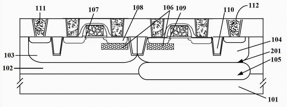
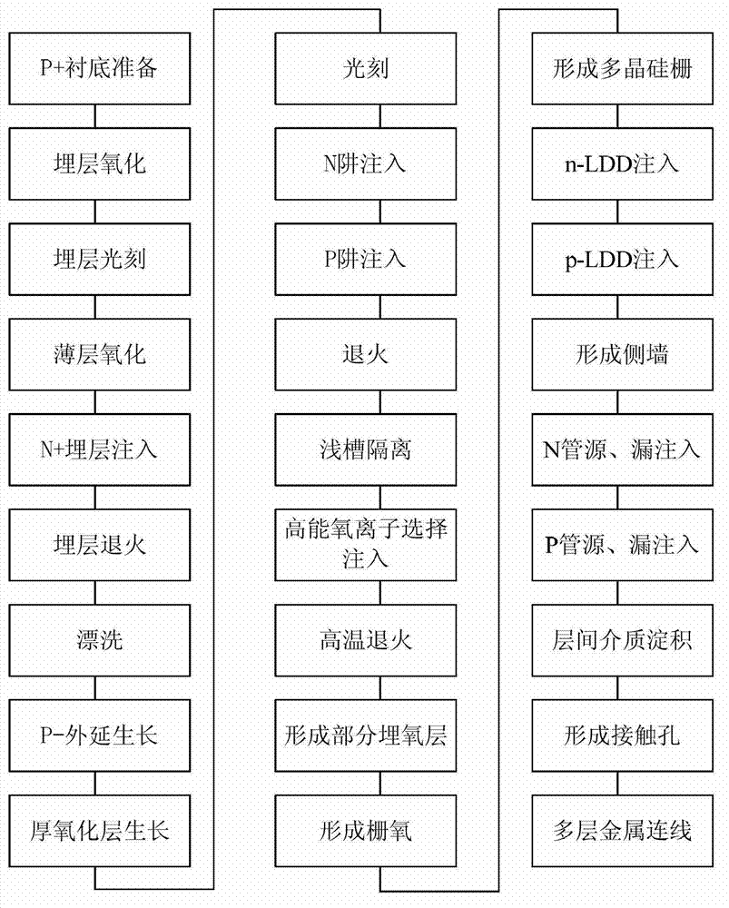
[0033] The substrate is a p+ type silicon wafer 101, doped with boron, with a concentration of 1e18cm -3 ; Doped with arsenic to form an n+ buried layer 105 with a thickness of 1 μm and a concentration of 6e18cm -3 ; An epitaxial layer 102 with a thickness of about 4.0 μm is epitaxially grown, boron-doped with a concentration of 1e16cm -3 ; Photolithography out of the N well region, the first dose is 5e13cm -2 , the energy is 2MeV phosphorus doping, and then the energy is 0.75MeV again, the dose is 5e12cm -2 Phosphorus doping; photoetching out the P well region, the first dose is 8e13cm -2 , boron doping with an energy of 1.5MeV, and then again with an energy of 0.3MeV and a dose of 6e12cm -2 Boron doping, followed by high-temperature annealing at 1100°C for 30 minutes to form a doped n-well 103 and a p-well 104 with a depth of 3 μm. The relationship between the concentration and depth of the p-well is as follows Figure 10 shown; complete deep trench isolation.

[0034] ...


PUM


Abstract

The invention relates to an anti-single-particle-radiation MOSFET (Metal-Oxide -Semiconductor Field Effect Transistor) apparatus and a preparation method, and relates to an integrated circuit technology. The anti-single-particle-radiation MOSFET apparatus comprises a high concentration substrate, source and drain regions, an epitaxial layer, an epitaxial layer abnormal well and an epitaxial layer isotypical well, wherein the wells are reversed doped wells; a part of oxygen burying layer is arranged below the drain region vertically; and a buried layer opposite to the epitaxial layer in type is arranged below the well in the same type of the epitaxial layer to form a PN node absorbing layer with a well boundary. The apparatus has the beneficial effects that the transient current impulse time width generated by the single particle is halved, and the impulse height is reduced to 40% of that of the original one. Compared with an SOI (Silicon on Insulator) apparatus, the self-heating effect and floating effect and the like can be effectively weakened.

Description

technical field [0001] The present invention relates to integrated circuit technology. Background technique [0002] The anti-single particle CMOS integrated circuit and its preparation method relate to the technical field of integrated circuits. [0003] With the development of space technology and nuclear technology, more and more electronic devices need to be applied in various radiation environments. At the same time, with the reduction of the feature size of integrated circuits, the increase of device frequency and the reduction of operating voltage, soft errors caused by single events have become one of the main problems affecting the reliability of integrated circuits. In particular, the transient current pulse (SET) caused by a single event hitting the sensitive node of the circuit will cause the logic circuit function to malfunction. In the transient current pulse effect, the time width of the current pulse is the most important parameter, so how to reduce the tra...

Claims


Application Information

Patent Timeline
Patent Type & Authority Applications(China)
IPC IPC(8): H01L27/092H01L29/06H01L21/8238
Inventor 翟亚红李平李威胡滨辜科
Owner UNIV OF ELECTRONICS SCI & TECH OF CHINA
Why Eureka
Try Eureka