Device and method for performing ultraviolet cleaning on nano-patterns

A nano-patterning and external cleaning technology, applied in cleaning methods and utensils, chemical instruments and methods, etc., can solve the problems of poor cleaning uniformity of silicon wafers, adverse effects, low ozone concentration, etc., and achieve good development and application prospects. Reduced energy consumption and uniform cleaning effect

Inactive Publication Date: 2013-03-20
INST OF MICROELECTRONICS CHINESE ACAD OF SCI
View PDF8 Cites 4 Cited by
  • Summary
  • Abstract
  • Description
  • Claims
  • Application Information

AI Technical Summary

Problems solved by technology

In view of this phenomenon, the existing ultraviolet cleaning device has not carried out relevant research on this phenomenon, so in the process of use, it faces the following problems: 1) the cleaning uniformity of the silicon wafer is not good; 2) the ozone c

Method used


Image

  • Device and method for performing ultraviolet cleaning on nano-patterns
  • Device and method for performing ultraviolet cleaning on nano-patterns

Examples


Embodiment Construction

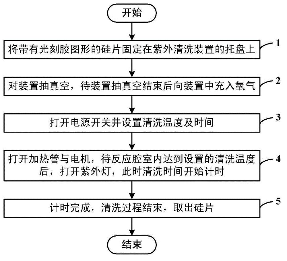
[0022] In order to make the object, technical solution and advantages of the present invention clearer, the present invention will be described in further detail below in conjunction with specific embodiments and with reference to the accompanying drawings.

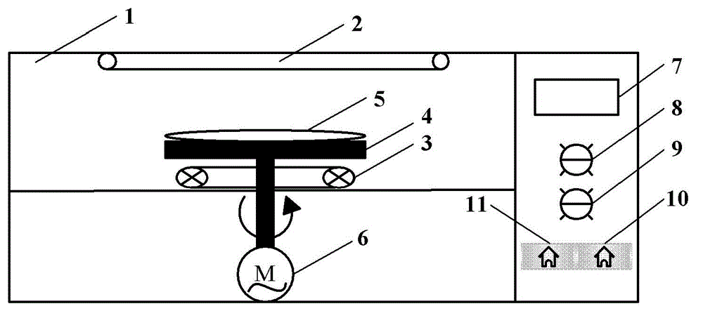
[0023] The realization principle of the present invention is firstly introduced below. After the CMOS process enters the 22ns node, there is no better way to remove the high molecular polymers that appear after electron beam lithography. Oxygen molecules in the air will also produce ozone and atomic oxygen after absorbing ultraviolet light. Under different bands of ultraviolet radiation, it is decomposed into atomic oxygen and oxygen, among which atomic oxygen is extremely active. Under its action, the high molecular polymer composed of carbon and hydrocarbons on the nanometer pattern can be decomposed into volatile gases . The invention controls the intensity and irradiation time of the ultraviolet rays and the surface ...


PUM


Abstract

The invention discloses a device and a method for performing ultraviolet cleaning on nano-patterns. The device comprises a reaction chamber (1), an ultraviolet lamp (2) arranged at the inner top of the chamber, a tray (4) which is arranged in the chamber and used for fixing a to-be-cleaned silicon wafer (5), a heating pipe (3) arranged below the tray, a motor (6) which is arranged at the bottom of the chamber, connected with the tray and used for driving the tray to rotate to uniformly clean the silicon wafer, and a control panel arranged on the outer side of the reaction chamber. According to the invention, oxygen gas is introduced to the device to increase the concentration of oxygen in the reaction chamber and can generate higher-density ozone under the action of ultraviolet irradiation, so as to completely remove high molecular polymer residues on the nano-patterns; and the rotating motor is arranged below the tray holding the silicon wafer to rotate the silicon wafer for heating and ultraviolet irradiation, so that the silicon wafer is uniformly heated by the heating pipe and uniformly irradiated with ultraviolet light, as a result, the cleaning effect is relatively uniform.

Description

technical field [0001] The invention relates to the technical field of cleaning nanoscale photoresist patterns in the semiconductor industry, in particular to a device and method for ultraviolet cleaning of nanometer patterns. Background technique [0002] In the semiconductor process, the cleaning technology has a great influence on the quality, precision and yield of the product. Traditional cleaning methods mostly use chemical cleaning and physical cleaning, which are difficult to meet the requirements of high cleanliness, safety and environmental protection in the semiconductor cleaning process. In order to solve the problems caused by traditional cleaning, the cleaning method widely used abroad is ultraviolet (UV) light cleaning. On the one hand, it can avoid the pollution caused by the use of organic solvents, and at the same time it can shorten the cleaning process. [0003] Ultraviolet light cleaning technology uses the photosensitive oxidation of organic compounds ...

Claims


Application Information

Patent Timeline
IPC IPC(8): B08B7/00
Inventor 赵士瑞景玉鹏于明岩郭晓龙徐昕伟
Owner INST OF MICROELECTRONICS CHINESE ACAD OF SCI
Why Eureka
Try Eureka