Structure and fabrication method of vertical junction-free gate-ring mosfet device

A junction ring and device technology, applied in semiconductor/solid-state device manufacturing, semiconductor devices, electrical components, etc., can solve problems such as insufficient gate control capability, excessive leakage current, difficult process realization, etc., and achieve the ability to resist short channel effects. The effect of strong, enhanced gate control capability and simple manufacturing process

A junction ring and device technology, applied in semiconductor/solid-state device manufacturing, semiconductor devices, electrical components, etc., can solve problems such as insufficient gate control capability, excessive leakage current, difficult process realization, etc., and achieve the ability to resist short channel effects. The effect of strong, enhanced gate control capability and simple manufacturing process

CN102983171BInactive Publication Date: 2015-10-28HARBIN ENG UNIV

Image

  • Structure and fabrication method of vertical junction-free gate-ring mosfet device
  • Structure and fabrication method of vertical junction-free gate-ring mosfet device
  • Structure and fabrication method of vertical junction-free gate-ring mosfet device

Examples


Embodiment Construction

[0022] The present invention is described in detail below in conjunction with accompanying drawing example:

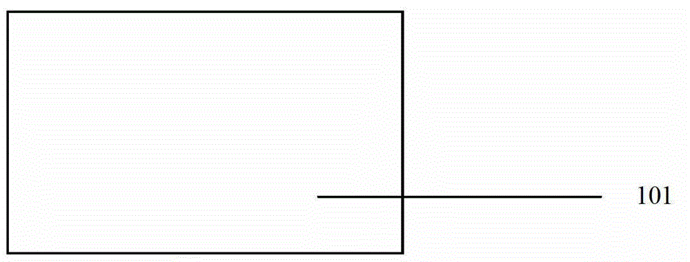
[0023] combine figure 2 . As shown, an n-type silicon wafer substrate 101 with crystal orientation is prepared with a thickness of 100 nm.

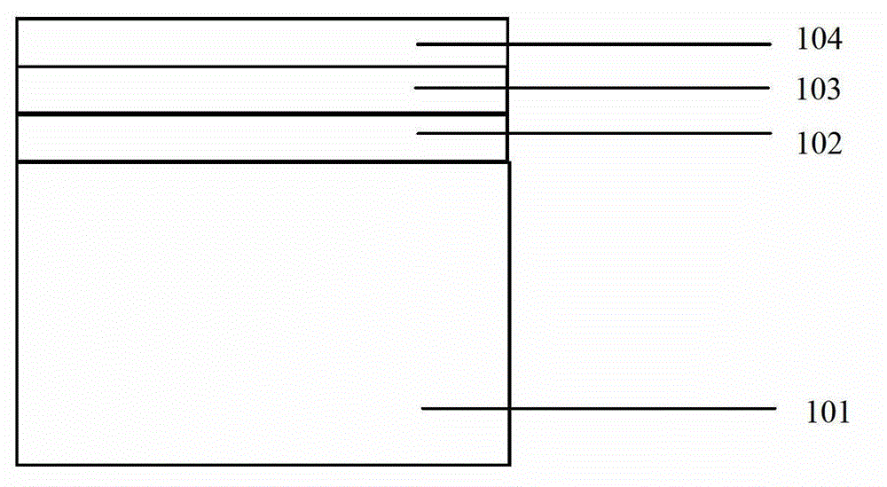
[0024] combine image 3 . On the n-type silicon wafer 101, SiO is sequentially deposited 2 layer 102, SiGe layer 103 and SiO 2 Layer 104. Of which SiO 2 layer 102, SiGe layer 103 and SiO 2 The thickness of the layer 104 is 20-50 nm.

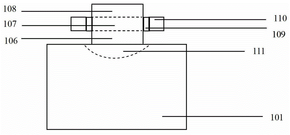
[0025] combine Figure 4 . right image 3 The structure is photolithographically made so that the middle part of the SiO 2 layer 102, SiGe layer 103 and SiO 2 Layer 104 is etched away in its entirety, forming a window. Then, the photoresist is used as a doping mask layer to perform n-type doping implantation on the silicon material, and rapid thermal annealing (RTA) activates the impurities to form the drain region 111 .

[0026] combine Figure 5 . An epitaxial silicon layer 105 i...


PUM


Abstract

The invention provides a structure and a manufacturing method of a vertical junctionless gate-all-round MOSFET (metal oxide semiconductor field effect transistor) device. The structure comprises a bottom-layer n-type silicon wafer substrate 101, wherein a drain region 111 is positioned at the lowest end of the device; a drain expansion region 106, a channel region 107 and a source region 108 grow on the substrate 101 epitaxially; a gate oxide layer 109 surrounds the whole channel region 107; and a polysilicon gate 110 is deposited on the gate oxide layer 109. Doping types and concentrations of the drain expansion region 106, the channel region 107, the source region 108 and the drain region 111 are the same; the doping types are n plus doping; the doping concentrations are 1*10<19>-8*10<19>cm<-3>; the doping type of the polysilicon gate 110 is p plus doping; and the doping concentration of the polysilicon gate 110 is 5*10<19>cm<-3>. The structure of the vertical junctionless gate-all-round MOSFET device can effectively inhibit action of a short channel effect. The invention also provides the manufacturing method of the vertical junctionless gate-all-round MOSFET device, which can simplify the technological process and allow the length of a gate and the thickness of a silicon region to be controlled flexibly.

Description

technical field [0001] The invention relates to a semiconductor device, and the invention also relates to a method for forming the semiconductor device. Specifically, it is a structure of a vertical junction-free ring gate MOSFET device and a manufacturing method thereof. Background technique [0002] In recent years, with the rapid development of the semiconductor industry, integrated circuits have developed into very large scale integrated circuits (ULSI) stage. The size of the device is also reduced to the nanometer level, which poses a great challenge for the development of new device structures and fabrication processes. Over the past few decades, the size of MOSFET devices has been continuously reduced, and today the effective channel length of MOSFET devices is less than 10 nanometers. Therefore, it is very difficult to form source / drain junctions and extremely high doping concentration gradients in short-channel devices. Based on the greatly increased cost and com...

Claims


Application Information

Patent Timeline
28 Oct 2015
Publication
CN102983171B
IPC
H01L29/78; H01L29/423; H01L29/10; H01L21/336; H01L21/28
Inventors
王颖; 单婵