Low-consumption low-minor lobe high-gain planar frequency scan antenna
A technology of frequency scanning antenna and low side lobe, applied in the direction of antenna, antenna coupling, antenna array, etc., can solve the problems of different array distribution, large transmission loss, large fluctuation of frequency band gain, etc., and achieve easy realization of amplitude distribution control, Convenient and easy to achieve, high design flexibility effect
- Summary
- Abstract
- Description
- Claims
- Application Information
AI Technical Summary
Problems solved by technology
Method used
Image
Examples
Embodiment 1
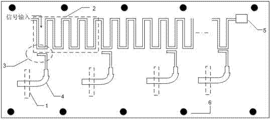
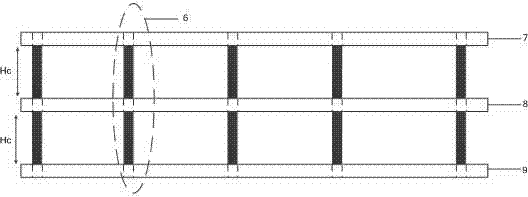
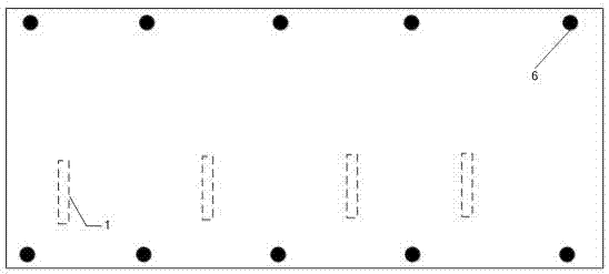
[0029] A low-consumption, low-sidelobe, high-gain planar frequency scanning antenna is composed of three planar dielectric substrates, the three planar dielectric substrates are arranged overlappingly, and there is an interval between each planar dielectric substrate, and the three planar dielectric substrates are passed through plastic screws 6 Fixed, wherein the first layer of planar dielectric substrate 7 includes the antenna radiation unit and the floor, and the upper and lower surfaces of the second layer of planar dielectric substrate 8 are symmetrically arranged, including a slow wave serpentine line structure 2, a coupling power divider 3, and a transmission line feed structure 4. Matching load 5, the end of the slow-wave serpentine line structure 2 is connected to the matching load 5, the slow-wave serpentine line structure 2 is coupled and connected to the coupling power divider 3, and the transmission line feed structure 4 is connected to the coupling power divider 3,...
Embodiment 2
[0039] It consists of three layers of planar dielectric substrates, the three layers of planar dielectric substrates are arranged overlappingly, and there is an interval between each layer of planar dielectric substrates, and the three layers of planar dielectric substrates are fixed by plastic screws 6, wherein the first layer of planar dielectric substrates 7 includes antenna radiation The unit and the floor, the upper and lower surfaces of the second plane dielectric substrate 8 are symmetrically arranged, including the slow wave serpentine line structure 2, the coupling power divider 3, the transmission line feed structure 4, the matching load 5, and the slow wave serpentine line structure 2 The end is connected to the matching load 5, the slow wave serpentine line structure 2 is coupled and connected to the coupling power divider 3, the transmission line feed structure 4 is connected to the coupling power divider 3, and the third plane dielectric substrate 9 is the floor. ...
Embodiment 3
[0045] It consists of three layers of planar dielectric substrates, the three layers of planar dielectric substrates are arranged overlappingly, and there is an interval between each layer of planar dielectric substrates, and the three layers of planar dielectric substrates are fixed by plastic screws 6, wherein the first layer of planar dielectric substrates 7 includes antenna radiation The unit and the floor, the upper and lower surfaces of the second plane dielectric substrate 8 are symmetrically arranged, including the slow wave serpentine line structure 2, the coupling power divider 3, the transmission line feed structure 4, the matching load 5, and the slow wave serpentine line structure 2 The end is connected to the matching load 5, the slow-wave serpentine line structure 2 is coupled to the coupling power divider 3, the transmission line feed structure 4 is connected to the coupling power divider), and the third layer of planar dielectric substrate 9 is the floor.
[00...
PUM
 Abstract
Description
Claims
Application Information
 - R&D
- Intellectual Property
- Life Sciences
- Materials
- Tech Scout
- Unparalleled Data Quality
- Higher Quality Content
- 60% Fewer Hallucinations
Browse by: Latest US Patents, China's latest patents, Technical Efficacy Thesaurus, Application Domain, Technology Topic, Popular Technical Reports.
© 2025 PatSnap. All rights reserved.Legal|Privacy policy|Modern Slavery Act Transparency Statement|Sitemap|About US| Contact US: help@patsnap.com


