Packaging structure and manufacture method for complementary metal-oxide-semiconductor transistor (CMOS) image sensors

An image sensor and packaging structure technology, applied in radiation control devices and other directions, can solve the problems of delamination of glass and silicon substrate, inability to use cost wafer-level processing and surface mounting technology, etc., to improve product reliability and production Efficiency, warpage improvement, cost reduction effect

Inactive Publication Date: 2013-03-27
BEIJING UNIV OF TECH
View PDF4 Cites 32 Cited by
  • Summary
  • Abstract
  • Description
  • Claims
  • Application Information

AI Technical Summary

Problems solved by technology

Third, the package structure shown cannot be used with lower cost wafer-level processing and surface mount technologies
For the CIS packaging structure

Method used


Image

  • Packaging structure and manufacture method for complementary metal-oxide-semiconductor transistor (CMOS) image sensors
  • Packaging structure and manufacture method for complementary metal-oxide-semiconductor transistor (CMOS) image sensors
  • Packaging structure and manufacture method for complementary metal-oxide-semiconductor transistor (CMOS) image sensors

Examples


Embodiment Construction

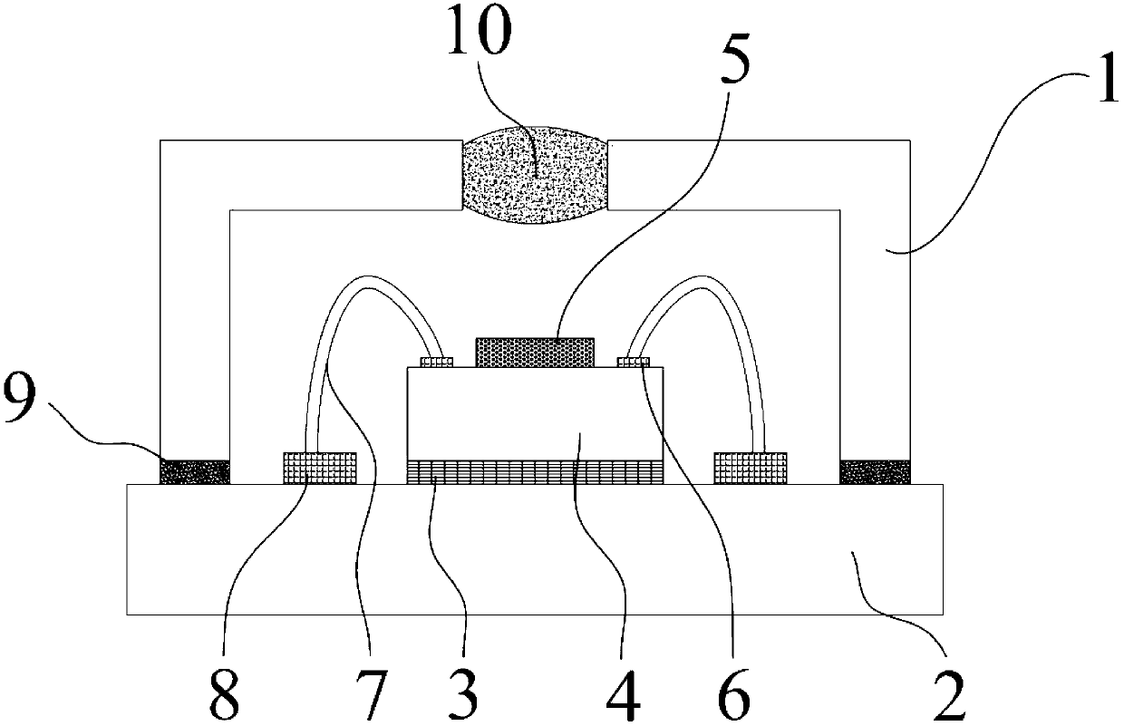
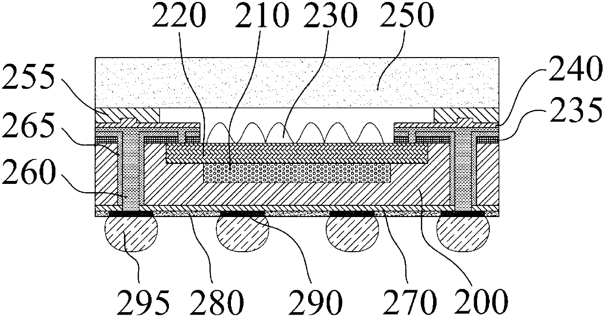
[0038] The present invention enhances the bonding force between the glass sheet 250 and the silicon substrate 200 by making a stepped protrusion or groove structure on the first surface 201 of the silicon substrate 200, and improves the delamination problem between the glass and the silicon substrate , which improves the reliability of the package and is suitable for CMOS image sensor (CIS) packages with larger chip sizes. figure 2 It is a schematic diagram of a CIS package of a stepped protrusion structure fabricated on the first surface 201 of the silicon substrate 200 according to an embodiment of the present invention.

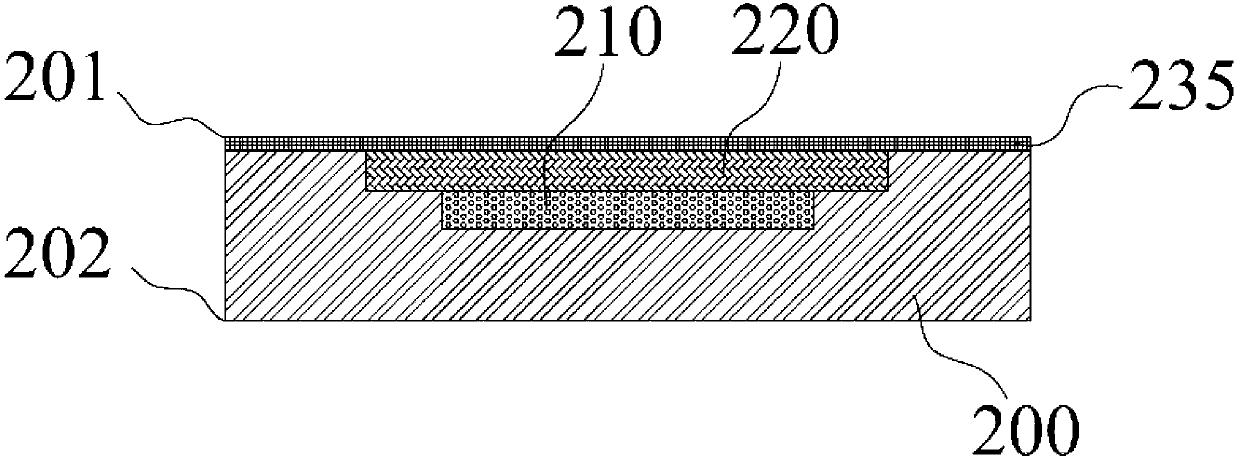
[0039] by figure 2 As shown, the CMOS image sensor (CIS) according to the embodiment of the present invention includes: a silicon substrate 200, and the front side of the silicon substrate 200 is a first surface 201 formed with a microlens 230, a metal interconnection layer 220 and an optical interaction region 210 , the back surface of the silicon subs...


PUM


Abstract

The invention discloses a packaging structure and a manufacture method for CMOS image sensors, and belongs to the sensor field. An optical interaction area is placed at a center on a first surface on the front surface of a silicon substrate, a metal interconnection layer is formed on the optical interaction area, a micro lens array is placed on the metal interconnection layer, and a first protection layer is arranged on the outer side of the metal interconnection layer; silicon through holes not penetrating through the silicon substrate and a redistribution layer are manufactured on the first surface, and an input/output (I/N) around the optical interaction area is connected with the silicon through holes through the redistribution layer; passivation layers are manufactured on the silicon through hole walls, and the silicon through holes are filled; a second protection layer is arranged on the redistribution layer; the silicon substrate is bonded with a glass sheet, and a cavity is arranged between the glass sheet and the silicon substrate; the second surface of the silicon substrate is thinned to expose the silicon through holes; a line layer is manufactured on the second surface of the silicon substrate to connect the silicon through holes to pads, and a solder mask layer is manufactured on the line layer and exposes the pads; and solder balls are arranged on the pads. According to the packaging structure and the manufacture method for CMOS image sensors, the layering problem between the glass and the silicon substrate in the packaging structure is solved, the reliability is improved, and the packaging structure is suitable for chips with large sizes.

Description

technical field [0001] The invention relates to the technical field of manufacturing semiconductor components. The invention provides a package structure of a CMOS image sensor and a manufacturing method of the CMOS image sensor. Background technique [0002] Image sensors belong to the optoelectronic components category in the optoelectronic industry. It is a semiconductor module and a device that converts an optical image into an electronic signal. The electronic signal can be used for further processing or digitized and stored, or used to transfer the image to another display device for display, etc. It is widely used in digital cameras and other electro-optical devices. Image sensors are now mainly divided into charge-coupled devices (CCD) and CMOS image sensors (CIS, CMOSImageSensor). Although CCD image sensors are superior to CMOS image sensors in terms of image quality and noise, CMOS sensors can be manufactured with traditional semiconductor production techniques ...

Claims


Application Information

Patent Timeline
IPC IPC(8): H01L27/146
Inventor 秦飞武伟安彤刘程艳陈思夏国峰朱文辉
Owner BEIJING UNIV OF TECH
Why Eureka
Try Eureka