Super-luminescent diode and method for manufacturing same

A technology of superluminescence and manufacturing method, which is applied in the field of active semiconductor light-emitting devices, and can solve problems such as difficult process realization, low fiber output power, small ripple coefficient, etc., achieve high optical output power and fiber coupling efficiency, and reduce process Achieve Difficult, Low Polarization Sensitivity Effects

Active Publication Date: 2013-04-03
WUHAN HUAGONG GENUINE OPTICS TECH
View PDF4 Cites 17 Cited by
  • Summary
  • Abstract
  • Description
  • Claims
  • Application Information

AI Technical Summary

Problems solved by technology

[0003] The active region of a traditional superluminescent light-emitting diode is generally a bulk material or a compressively strained multiple quantum well. The output power of the TE mode (te mode) is generally much greater than that of the TM mode (tm mode). In order to ensure that the linear polarization direction of light remains unchanged , need to use polarization-maintaining fiber or other polarization control devices to adjust in applications such as fiber optic sensing, which increases the cost of use
[0004] In addition, because the large spectral ripple will produce a secondary coherence peak, which affects the accuracy of the fiber optic gyroscope, it is generally required that the superluminescent light-emitting diode has a small ripple coefficient
[0005] The methods to obtain lower spectral ripple generally include making the absorption area on the backlight surface, adopting an inclined strip structure in the gain area, and coating the light-emitting end surface with anti-reflection coating, etc., but these methods have high requirements on the end surface coating process, and the process is difficult to realize. Larger, and it is not easy to obtain higher optical output power
[0006] In the design of the waveguide structure of superluminescent tubes, the ridge waveguide structure is usually used, which has the advantages of simple process and good reliability, but the large far-field divergence angle in the material growth direction makes the fiber coupling power loss large. Low fiber output power

Method used


Image

  • Super-luminescent diode and method for manufacturing same
  • Super-luminescent diode and method for manufacturing same
  • Super-luminescent diode and method for manufacturing same

Examples


Embodiment Construction

[0039] The present invention will be further described below in conjunction with the accompanying drawings and specific embodiments, so that those skilled in the art can better understand the present invention and implement it, but the examples given are not intended to limit the present invention.

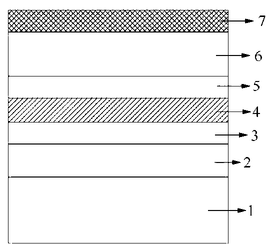
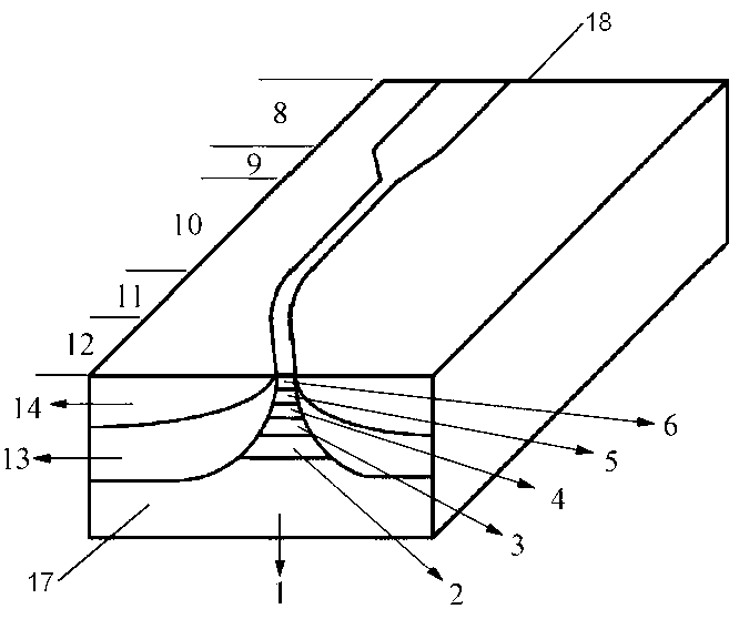
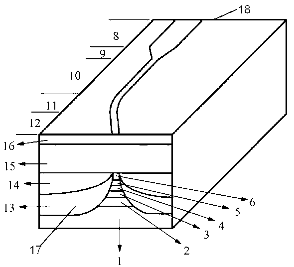
[0040] like image 3 As shown, it is an embodiment of a superluminescent light-emitting diode of the present invention, including a substrate, and a buffer layer, a lower confinement layer, an active region, an upper confinement layer, a cladding layer, and a cladding layer are sequentially arranged on the substrate and the contact layer.

[0041] The two ends of the super-radiant light-emitting diode are respectively a backlight end 18 and a light-emitting end 17, and the backlight end 18 is provided with an absorption region 8 for absorbing light reflected by the light-emitting end 17, and the light-emitting end 17 is provided with a curved waveguide structure, so The curved wa...


PUM


Abstract

The invention discloses a super-luminescent diode and a method for manufacturing the same. The super-luminescent diode comprises a substrate. The method includes sequentially forming a buffer layer, a lower limiting layer, an active region, an upper limiting layer and a first p-type covering layer on the substrate so as to form a primary epitaxial slice by an epitaxial growth technology; sequentially growing a second p-type covering layer and an n-type covering layer on the surface of the primary epitaxial slice so as to form a secondary epitaxial slice by the epitaxial growth technology; growing a covering layer and a contact layer on the surface of the secondary epitaxial slice so as to form a tertiary epitaxial slice by the epitaxial growth technology; and manufacturing the tertiary epitaxial slice into a super-luminescent diode chip by photoetching, etching, slice grinding and sputtering processes sequentially, and coating an antireflection film on a light emergent end surface of the chip. The super-luminescent diode and the method have the advantages of low polarization sensitivity and ripple coefficient, high power, wide spectrum and the like.

Description

technical field [0001] The invention belongs to the technical field of active semiconductor light-emitting devices, and in particular relates to a superluminescent light-emitting diode. Background technique [0002] Superluminescent light-emitting diode is a device that spontaneously amplifies radiated light. Its photoelectric characteristics are between lasers and light-emitting diodes. It has the advantages of high output power of lasers and wide-spectrum characteristics of light-emitting diodes. Tomography imaging technology and optical fiber communication have a wide range of applications. [0003] The active region of a traditional superluminescent light-emitting diode is generally a bulk material or a compressively strained multiple quantum well. The output power of the TE mode (te mode) is generally much greater than that of the TM mode (tm mode). In order to ensure that the linear polarization direction of light remains unchanged , it is necessary to use polarizatio...

Claims


Application Information

Patent Timeline
Patent Type & Authority Applications(China)
IPC IPC(8): H01S5/34H01S5/20
Inventor 周志强刘建军唐琦
Owner WUHAN HUAGONG GENUINE OPTICS TECH
Why Eureka
Try Eureka