Waveguide coupler with echelon grating mirror and preparation method thereof

A kind of echelle grating and reflector technology, applied in the coupling of optical waveguide, optical waveguide light guide, light guide, etc., can solve the problems of not meeting the requirements of optical communication, polarization-related loss, large device size, etc., and reduce the spatial orientation of the beam And the effect of extremely high position, reduced energy loss, and large alignment tolerance

Inactive Publication Date: 2013-04-10
SOUTHEAST UNIV
View PDF2 Cites 12 Cited by
  • Summary
  • Abstract
  • Description
  • Claims
  • Application Information

AI Technical Summary

Problems solved by technology

However, based on the large size of the SoS waveguide, there are disadvantages: the height of the waveguide is difficult to realize in the process, and due to the large etching depth, it is easy to cause the side etching to be non-perpendicular, resulting in multimode waveguide and polarization-dependent loss; the large waveguide width leads to device size Larger, not conducive to integration
The most widely used in practice is the wedge-shaped optical waveguide coupler.

Method used


Image

  • Waveguide coupler with echelon grating mirror and preparation method thereof
  • Waveguide coupler with echelon grating mirror and preparation method thereof
  • Waveguide coupler with echelon grating mirror and preparation method thereof

Examples


preparation example Construction

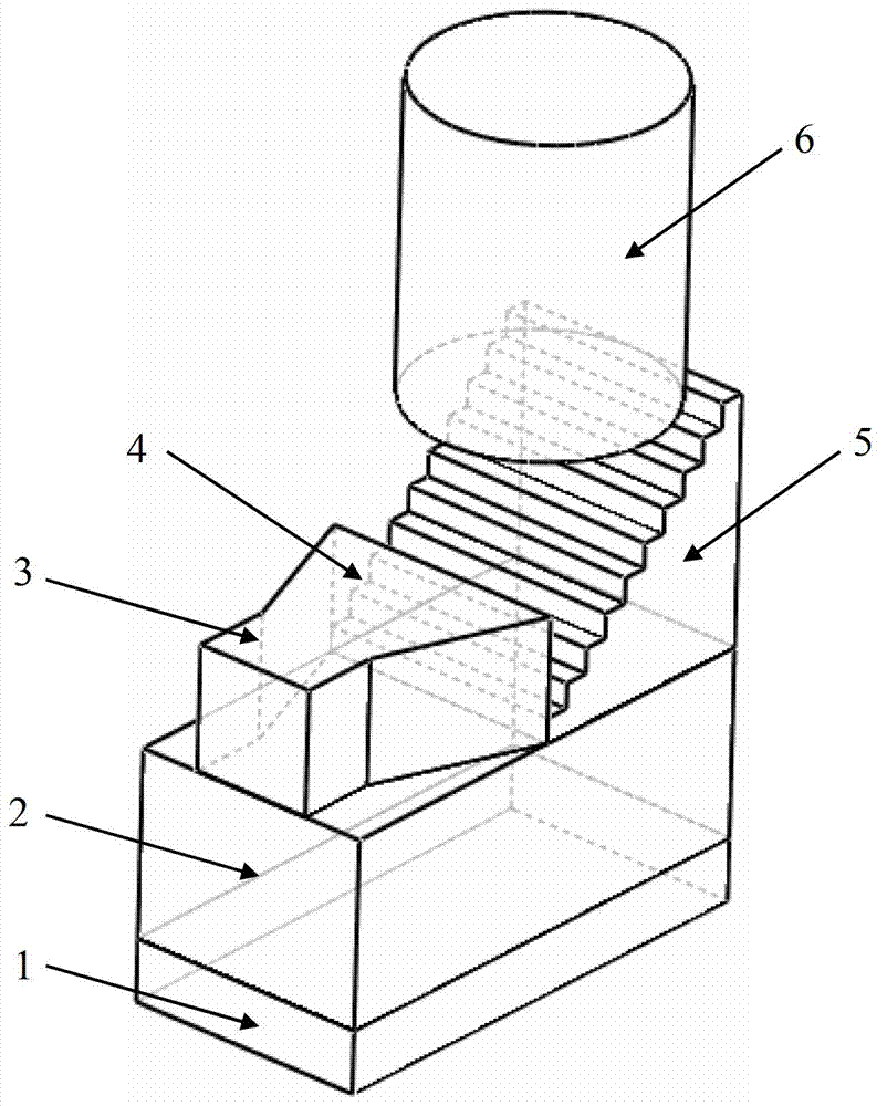
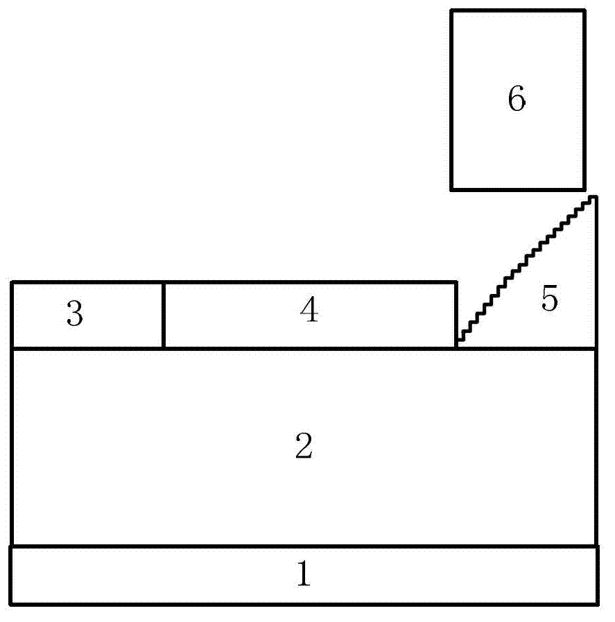
[0030] The above-mentioned preparation method of the waveguide coupler with the stepped grating reflector comprises the following steps:

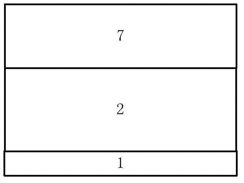
[0031] Step 10): Take a silicon substrate 1, and prepare a silicon dioxide buffer layer 2 with a thickness of 15 μm to 20 μm on the silicon substrate 1; Growth doped germanium dioxide (GeO 2 ) silicon dioxide to form a waveguide layer 7 with a thickness of 6 μm-10 μm, and the refractive index of the waveguide layer 7 is higher than that of the buffer layer 2 .

[0032] Step 20): On the waveguide layer 7, the photolithography and etching processes are repeatedly used to prepare the grating reflector 5.

[0033]In step 20), the photolithography refers to copying the pattern of the mask onto the waveguide layer 7, and after each photolithography, an etching process is performed respectively to prepare the grating reflector 5.

[0034] Step 30): On the waveguide layer 7, the tapered waveguide 4 is prepared by photolithography and etching.

...

Embodiment

[0038] A preparation method of a polarization-maintaining planar lightwave optical path is introduced below to describe the above preparation method in more detail.

[0039] Step 10): making the silicon dioxide buffer layer 2 and the waveguide 7 . refer to image 3 As shown, firstly, the silicon wafer, that is, the substrate 1, is cleaned by wet chemical method to remove the dirt on the surface; then, after ultrasonic cleaning and drying of deionized water, the cleaning of the silicon wafer is completed; next, the silicon dioxide buffer is prepared Layer 2, there are many methods for preparing the silica buffer layer 2, such as chemical vapor deposition (CVD), flame hydrolysis (FHD), sol-gel (Sol-Gel), thermal oxidation (TO) and so on. Since the thermal oxidation method can oxidize more than one hundred silicon wafers at the same time, it has higher efficiency in actual production, and can simultaneously oxidize the front and back sides of the silicon substrate 1, thereby eli...


PUM

PropertyMeasurementUnit
Thicknessaaaaaaaaaa

Abstract

The invention discloses a waveguide coupler with an echelon grating mirror which comprises a substrate, a buffer layer, a waveguide, a tapered waveguide, the echelon grating mirror and an optical fiber. A reflecting face of the echelon grating mirror is provided with echelon grating. The buffer layer is fixedly connected with the top face of the substrate. The waveguide, the tapered waveguide and the echelon grating mirror are fixedly connected with the top face of the buffer layer. The height of the tapered waveguide is equal to that of the waveguide. One end of the tapered waveguide is a narrow end, and the other end of the tapered waveguide is a wide end. The narrow end of the tapered waveguide is fixedly connected with an input end of the waveguide, and the wide end of the tapered waveguide is opposite to the reflecting face of the echelon grating mirror. The optical fiber is arranged vertically and arranged above the echelon grating mirror, and an output end of the optical fiber is opposite to the reflecting face of the echelon grating mirror. The waveguide coupler is capable of enabling the optic fiber and the waveguide to achieve high-efficiency coupling and provided with high alignment tolerance. Meanwhile, the invention further discloses a preparation method of the waveguide coupler. The preparation method is simple and compatible with a metal oxide semiconductor (MOS) technology.

Description

technical field [0001] The invention belongs to the technical field of integrated photonic devices, and in particular relates to a waveguide coupler with a stepped grating reflector and a preparation method thereof. Background technique [0002] With the continuous development of silicon-based materials in the field of integrated photonics, silicon-based photonic devices have been widely used. The mainstream development trend of integrated photonic optical circuits is miniaturization and integration of photonic devices. Silicon-based silica (silicon-based silica: English full name: Silica on Silicon, abbreviation: SoS in the text) waveguide material has a refractive index similar to that of optical fiber, and there is no refractive index mismatch problem. At present, there is no coupling problem between passive optical devices and optical fibers based on large-scale SoS waveguides, and they have been commercialized, such as SoS waveguide optical splitters based on a cross-s...

Claims


Application Information

Patent Timeline
IPC IPC(8): G02B6/122G02B6/13G02B6/136G02B6/24
Inventor 孙小菡蒋卫锋柏宁丰刘旭吴晨
Owner SOUTHEAST UNIV
Why Eureka
Try Eureka