Radio frequency horizontal double-diffusion-field effect transistor and manufacturing method thereof

A field effect transistor, lateral double diffusion technology, applied in semiconductor/solid-state device manufacturing, semiconductor devices, electric solid-state devices, etc., can solve the evaluation of device reliability, poor quality and other problems, achieve simple preparation process, enhanced durability sexual effect

Active Publication Date: 2013-04-10
SHANGHAI HUAHONG GRACE SEMICON MFG CORP
View PDF8 Cites 4 Cited by
  • Summary
  • Abstract
  • Description
  • Claims
  • Application Information

AI Technical Summary

Problems solved by technology

[0004] At present, under normal circumstances, the oxide layer under the Faraday shielding layer prepared by this method is grown by

Method used


Image

  • Radio frequency horizontal double-diffusion-field effect transistor and manufacturing method thereof
  • Radio frequency horizontal double-diffusion-field effect transistor and manufacturing method thereof
  • Radio frequency horizontal double-diffusion-field effect transistor and manufacturing method thereof

Examples


Embodiment Construction

[0057] In order to enable your examiners to have a further understanding and understanding of the purpose, features and effects of the present invention, the following detailed description is as follows with the accompanying drawings.

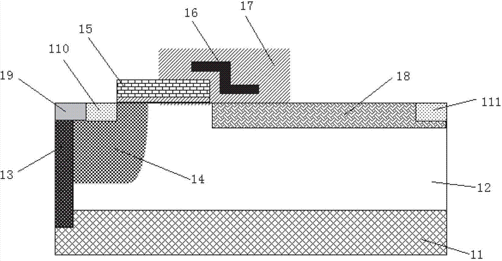
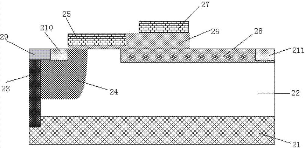
[0058] Such as figure 2As shown, it is a schematic structural diagram of the first embodiment of the RFLDMOS device of the present invention, wherein a substrate doped with high-concentration P-type impurities is used, that is, a P+ substrate 21. According to different requirements for device withstand voltage, on the P+ type substrate 21 , grow P-type epitaxial layers 12 with different thicknesses and doping concentrations; define by photoresist, perform ion implantation to form lightly doped drift region 28; then grow a thicker oxide layer by thermal oxygen, then define and All or part of the oxide layer under the source terminal and the gate is removed, and then a thermal oxygen process is performed to grow a thinner oxide layer to make it ...


PUM

PropertyMeasurementUnit
Thicknessaaaaaaaaaa
Thicknessaaaaaaaaaa

Abstract

The invention discloses a radio frequency horizontal double-diffusion-field effect transistor comprising a polysilicon gate and a faraday shielding layer which is a polysilicon faraday shielding layer. The radio frequency horizontal double-diffusion-field effect transistor adopts a polysilicon faraday shielding layer structure. Compared with a traditional preparation technology of a faraday shielding payer, the preparation technology of the polysilicon faraday shielding layer is simple, a thermal oxidation process is added once, and an oxide layer deposition and metal deposition and corrosion process below the faraday shielding layer is reduced once. Quality of an oxide layer, prepared by the method, below the faraday shielding layer grows better than quality of a normal faraday shielding layer which grows through a deposition way, and therefore durability of a component is enhanced. Compared with a component of the normal faraday shielding layer, the component of the radio frequency horizontal double-diffusion-field effect transistor has the advantages of being same in breakdown voltage and on-resistance and the like. A step gate structure prepared by the method can also play a role in preventing infusion (host controller interface (HCI)) of hot carriers.

Description

technical field [0001] The invention relates to a semiconductor integrated circuit, in particular to a radio frequency lateral double-diffusion field effect transistor, and also relates to a manufacturing method of the transistor. Background technique [0002] With the advent of the 3G era, more and more communication fields require the development of more powerful radio frequency (RF) devices. Radio Frequency Lateral Double Diffused Field Effect Transistor (RFLDMOS), due to its very high output power, has been widely used in portable wireless base station power amplification as early as the 1990s, and its application frequency is 900MHz-3.8GHz. Compared with traditional silicon-based bipolar transistors, RFLDMOS has better linearity, higher power and gain. Today, RFLDMOS is more popular than bipolar, and GaAs devices. [0003] The current structure of RFLDMOS is as follows figure 1 As shown, a substrate doped with a high-concentration P-type impurity, that is, a P-type s...

Claims


Application Information

Patent Timeline
IPC IPC(8): H01L29/78H01L23/60H01L21/336
CPCH01L29/7835H01L29/1045H01L29/402
Inventor 李娟娟钱文生韩峰慈朋亮
Owner SHANGHAI HUAHONG GRACE SEMICON MFG CORP
Why Eureka
Try Eureka