Ultra-large size flat panel display maskless photolithography system and method

An exposure system and maskless technology, which is applied in the field of maskless direct writing digital lithography, can solve the problems of poor exposure quality, expensive patterned mask or film, long procurement and delivery time of optical masks, etc.

Active Publication Date: 2013-04-17
ZHONGSHAN AISCENT TECH
View PDF13 Cites 26 Cited by
  • Summary
  • Abstract
  • Description
  • Claims
  • Application Information

AI Technical Summary

Problems solved by technology

Basically these very heavy quartz masks cost over $1 million
[0009] And in traditional mask lithography, patterned masks or films for high-resolution applications are usually very expensive and have a short lifetime
In addition, optical mask plates require a long procurement lead time, which is a problem for products that need to be developed in a short period of time
If a particular retic

Method used


Image

  • Ultra-large size flat panel display maskless photolithography system and method
  • Ultra-large size flat panel display maskless photolithography system and method
  • Ultra-large size flat panel display maskless photolithography system and method

Examples


Embodiment Construction

[0055] The following will clearly and completely describe the technical solutions in the embodiments of the present invention with reference to the drawings in the embodiments of the present invention. Obviously, the described embodiments are part of the embodiments of the present invention, not all of them. Based on the embodiments of the present invention, all other embodiments obtained by persons of ordinary skill in the art without making creative efforts shall fall within the protection scope of the present invention.

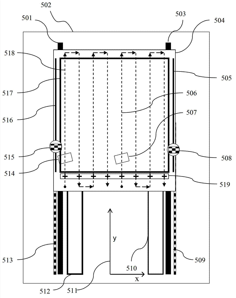
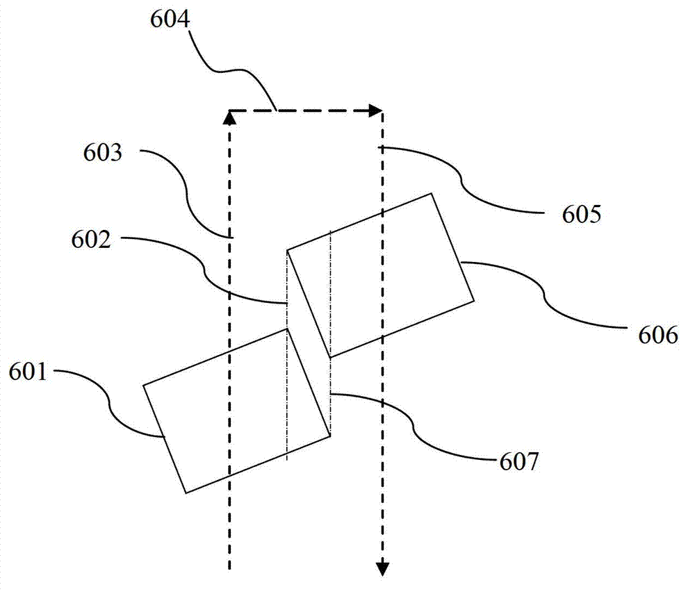
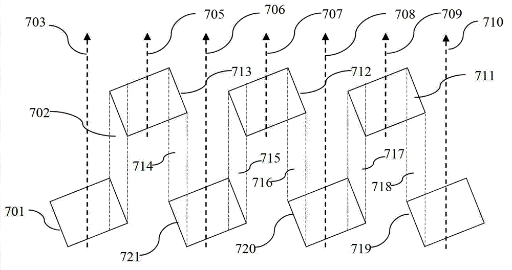
[0056] It should be understood that the present invention relates to maskless lithography or direct-write digital imaging technology, and in particular to a single-sided maskless exposure system or a double-sided maskless exposure system capable of performing simultaneous imaging on one or both sides of a flat panel. Exposure, the flat plate is, for example, a substrate for a printed circuit board (PCB), or a sheet for a lead frame. The main application sc...


PUM


Abstract

A maskless exposure system that has multiple maskless optical engines arranged in an (NM) matrix that form and project a pattern onto a substrate. A first stage system is capable of driving the maskless optical engines in a first direction, a second stage system capable of holding and moving the substrate in a second direction perpendicular to the first direction. A control system that processes data and synchronizing movement of the first and second stage systems and a vision system that detects the positions of the second stage system to synchronize movements with the multiple optical engines.

Description

technical field [0001] The invention relates to a maskless direct writing digital photolithography technology, in particular to a maskless exposure system, a maskless exposure method, a component manufacturing method and an image scanning method. Background technique [0002] Flat panel display (FPD) substrates have been widely used in personal computers, televisions, etc. This liquid crystal display (LCD) substrate is fabricated by photolithographically preparing transparent thin-film electrodes on a photosensitive substrate. In order to achieve photolithography exposure, exposure instruments that project a template pattern onto a photoresist on a glass substrate through an optical projection system have been produced and used. [0003] Recently, it is expected that the area of ​​the flat panel display substrate will further increase. Correspondingly, the exposure area in the projection exposure device needs to be further increased. [0004] For large TFT-LCDs, it is usu...

Claims


Application Information

Patent Timeline
IPC IPC(8): G03F7/20
Inventor 梅文辉杜卫冲曲鲁杰
Owner ZHONGSHAN AISCENT TECH
Why Eureka
Try Eureka