Method for preparing silicon band by direct forming and silicon wafer direct forming device

A direct, silicon wafer technology, applied in chemical instruments and methods, self-melting liquid pulling method, crystal growth, etc., to achieve the effects of improving photoelectric conversion efficiency, improving purity, and process stability

Active Publication Date: 2016-04-27
SHANGHAI UNIV
View PDF8 Cites 0 Cited by
  • Summary
  • Abstract
  • Description
  • Claims
  • Application Information

AI Technical Summary

Problems solved by technology

[0004] In order to solve the problems of the prior art, the object of the present invention is to overcome the defects of the prior art, provide a method for preparing silicon strips by direct forming and a direct forming device for silicon wafers, constrain the solid-liquid interface in the forming process of silicon wafers, and then stabilize Control the shape of the solid-liquid interface, directly prepare strip silicon, eliminate the pollution of silicon melt during the production process, reduce the defects of silicon wafers, improve the photoelectric conversion efficiency of silicon wafers, and realize the industrial application of large-scale direct production of strip silicon

Method used


Image

  • Method for preparing silicon band by direct forming and silicon wafer direct forming device
  • Method for preparing silicon band by direct forming and silicon wafer direct forming device
  • Method for preparing silicon band by direct forming and silicon wafer direct forming device

Examples


Embodiment 1

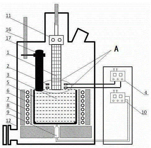
[0029] see Figure 1 ~ Figure 3, a silicon wafer direct forming device, comprising a silicon material melting and heat preservation device, a feeding device, a direct-draw dummy device 11 and a soft contact forming device with silicon, specifically: the silicon material melting and heat preservation device is a vacuum furnace, consisting of a quartz crucible 5, Insulation graphite cylinder 6, heating device 7, insulation graphite felt 8, thermocouple 9, temperature controller 10 and furnace shell 12 are composed, and heating device 7 adopts the mode of induction heating or resistance heating to heat, and heating device 7 is connected with the outside of vacuum furnace. The external power supply is connected, the thermocouple 9 is connected with the temperature controller 10 signal, the temperature of the quartz crucible 5 is detected in real time through the thermocouple 9, and the signal feedback is formed to the external power supply, and the heating output power of the heati...

Embodiment 2

[0034] This embodiment is basically the same as Embodiment 1, especially in that:

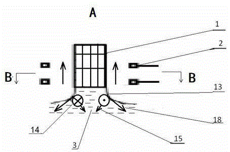
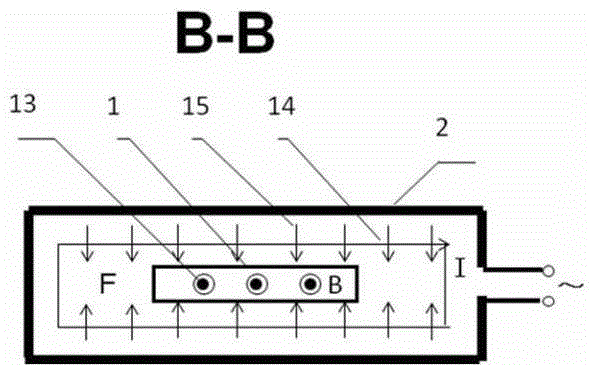
[0035] In this embodiment, the shape of the induction coil 2 is a special-shaped induction coil with a length-to-width ratio greater than 1 and a circular arc at both ends. The contact forming mechanism is established in the solid-liquid interface region 13, which is beneficial to direct directional solidification to form a silicon band with a uniform cross-section of the silicon wafer.


PUM

PropertyMeasurementUnit
thicknessaaaaaaaaaa
widthaaaaaaaaaa

Abstract

The invention discloses a method for preparing silicon tape by direct forming. An alternating magnetic field is applied to the solid-liquid interface region between a silicon wafer and a silicon melt, and an induced current is formed in the silicon melt at the front of the solid-liquid interface. The joint effect of magnetic field and induced current forms a vertical solid-liquid interface at the solid-liquid interface and points to the electromagnetic extrusion force inside the silicon melt, and adjusts the magnitude of the electromagnetic extrusion force so that the electromagnetic extrusion force completely offsets the narrow edge of the silicon wafer The inward surface tension at the solid-liquid interface enables the flexible electromagnetic force to constrain and stabilize the shape of the solid-liquid interface, so that the silicon melt constrained by the flexible electromagnetic force is shaped and continuously solidified, and then the solidified strip-shaped silicon slab continues Pull out, directly prepared with silicon. The invention also discloses a silicon wafer direct forming device, which includes a silicon material melting and heat preservation device, a feeding device, a direct pulling dummy device and a silicon-taped soft-contact forming device, which can directly prepare a silicon wafer, realize clean production, and reduce silicon wafer defects. Realize large-scale direct production of industrial applications with silicon.

Description

technical field [0001] The invention relates to a photovoltaic material preparation process and device, in particular to a silicon material preparation process and device, which are applied to the preparation of solar-grade silicon bands. Background technique [0002] Today, with the rapid development of photovoltaic technology and micro-semiconductor inverter technology, solar cells produced by silicon crystals can directly convert solar energy into light energy, realizing the beginning of a green energy revolution. The silicon wafers used in traditional solar cells are cut from silicon ingots. Due to the limitations of the current wire saw technology, about 30% of the silicon material will be lost when the silicon ingots are processed into silicon blocks, and silicon blocks are processed into silicon wafers. 34-50% of the silicon material will be lost, and the cut silicon wafers need to be inspected and screened, and subsequent processes will also cause losses. Therefore,...

Claims


Application Information

Patent Timeline
Patent Type & Authority Patents(China)
IPC IPC(8): C30B15/36C30B15/22C30B29/06
Inventor 钟云波沈喆黄靖文龙琼孙宗乾吴秋芳李甫周鹏伟董立城郑天祥
Owner SHANGHAI UNIV
Why Eureka
Try Eureka