Complementary metal oxide semiconductor (COMS) image sensor pixel structure and manufacturing method thereof
A technology of image sensor and pixel structure, which is applied in the direction of electrical components, electric solid-state devices, semiconductor devices, etc., can solve the problems of sensitivity, resolution and definition deterioration, chip performance deterioration, pixel optical crosstalk, etc., to achieve Effects of improving optical resolution and sensitivity, reducing length, and increasing light absorption
- Summary
- Abstract
- Description
- Claims
- Application Information
AI Technical Summary
Problems solved by technology
Method used
Image

Examples
no. 1 example
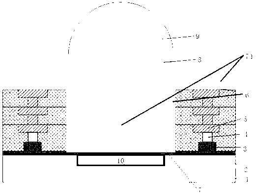
[0064] see figure 1 , in the first embodiment, the pixel structure of the CMOS image sensor includes a photodiode 10 and a multilayer structure (for standard CMOS device levels) on the silicon substrate 1, in this embodiment, the silicon substrate in this embodiment There is also a layer of gate oxide layer 2 between 1 and the multilayer structure, wherein the multilayer structure includes a polysilicon layer 3, a tungsten contact hole layer 4, a copper metal interconnection layer 5, and other through holes on it from bottom to top layers, metal interconnect layers, and interconnect dielectric layers. A deep groove 7 forming a light-transmitting space is formed above the photodiode 10 . The sidewall of the deep groove 7 is surrounded by a metal reflective layer 6 to reflect light incident on the metal reflective layer 6 . The metal reflective layer 6 is made of aluminum material with a thickness of 100A, and is prepared by PVD film forming technology.
[0065] Wherein, the d...
no. 2 example
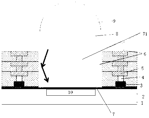
[0075] read on figure 2 , in the second embodiment, the pixel structure of the CMOS image sensor includes a photodiode 10 and a multilayer structure (for standard CMOS device levels) on the silicon substrate 1, in this embodiment, the silicon substrate in this embodiment There is also a layer of gate oxide layer 2 between 1 and the multilayer structure, wherein the multilayer structure includes a polysilicon layer 3, a tungsten contact hole layer 4, a copper metal interconnection layer 5, and other through holes on it from bottom to top layers, metal interconnect layers, and interconnect dielectric layers. There is a deep groove 7 forming a light-transmitting space above the photodiode 10, and the side walls of the deep groove 7 are surrounded by a metal reflective layer 6 to reflect light incident on the metal reflective layer 6; a layer is also prepared on the top layer of the multilayer structure. A metal reflective layer 6 is used to reflect light incident from the top o...
no. 3 example
[0083] see Figure 6 , the pixel structure of the CMOS image sensor includes a photodiode 37 and a multilayer structure (for standard CMOS device levels) on a silicon substrate 31, and there is also a layer between the silicon substrate 31 and the multilayer structure in this embodiment Gate oxide layer 32, wherein the multi-layer structure includes from bottom to top the first polysilicon layer 33, the W contact hole layer 34, the Cu metal interconnect layer 35 and the first via layer 351, the interconnect dielectric layer (not marked), a deep groove 38 is arranged above the photodiode 37, and a light reflection shielding layer 39 is also provided in the side wall medium of the deep groove 38, and the distance between the light reflection shielding layer 39 and the side wall of the deep groove 38 is 0.1um , it completely surrounds the deep trench 39, and it includes a second polysilicon layer 391, a second contact hole layer 392, and a second metal interconnection layer A tha...
PUM
| Property | Measurement | Unit |
|---|---|---|
| Thickness | aaaaa | aaaaa |
Abstract
Description
Claims
Application Information
 - R&D
- Intellectual Property
- Life Sciences
- Materials
- Tech Scout
- Unparalleled Data Quality
- Higher Quality Content
- 60% Fewer Hallucinations
Browse by: Latest US Patents, China's latest patents, Technical Efficacy Thesaurus, Application Domain, Technology Topic, Popular Technical Reports.
© 2025 PatSnap. All rights reserved.Legal|Privacy policy|Modern Slavery Act Transparency Statement|Sitemap|About US| Contact US: help@patsnap.com