Organic semiconductor material, and preparation method and application thereof
A technology of organic semiconductors and organic palladium, which is applied in semiconductor/solid-state device manufacturing, semiconductor devices, organic chemistry, etc., can solve the problems of short lifespan and low luminous efficiency, and achieve high production efficiency, low cost, luminous efficiency and heat dissipation. The effect of stability improvement
- Summary
- Abstract
- Description
- Claims
- Application Information
AI Technical Summary
Problems solved by technology
Method used
Image
Examples
preparation example Construction
[0023] The embodiment of the present invention further provides a method for preparing the above-mentioned organic semiconductor material, including the following steps:
[0024] Step S01, providing raw materials:
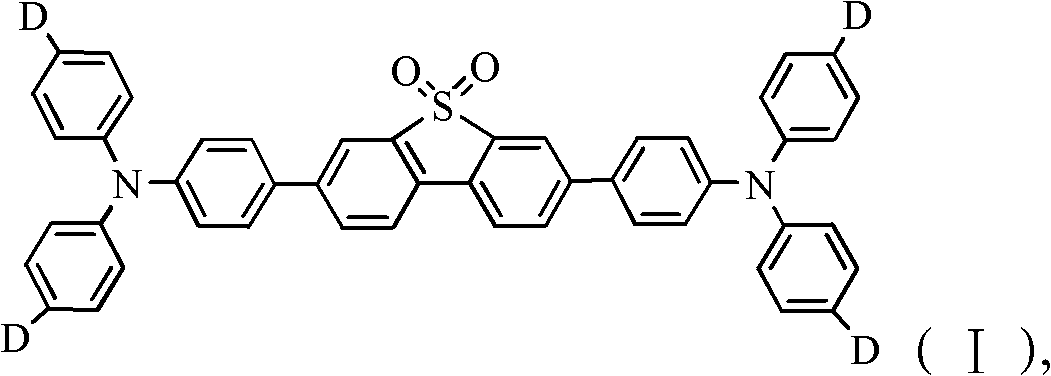
[0025] Provide the structural formula as Compound A, the structural formula is The compound B, wherein, D is selected from hydrogen atom (-H), alkyl (-R), alkoxyl (-OR);
[0026] Step S02, Suzuki reaction:
[0027] Compound A and Compound B with a molar ratio of 1:2 to 3 were dissolved in a catalyst and a basic organic solvent, and Suzuki reaction was carried out under anaerobic conditions and at a temperature of 60°C to 130°C for 20 hours to 40 hours to obtain the following: The organic semiconductor material of structural formula I, reaction formula is expressed as:
[0028]
[0029] Specifically, in step S01, compound A can be purchased from the market, or can be prepared by the following method:
[0030]
[0031] Dissolve dibenzothiophene sulfone i...
Embodiment 2
[0041] Example 2 of the present invention, 7-bis(4-(bis(4-tolyl)amine)phenyl)dibenzothiophene sulfone (DMPFSO) has the following structural formula:
[0042]
[0043] Example 2 of the present invention, the preparation method of 7-bis(4-(bis(4-tolyl)amine)phenyl)dibenzothiophene sulfone (DMPFSO) comprises the following steps:
[0044] Step 1, preparation of 2,7-dibromodibenzothiophene sulfone:
[0045] Dissolve 4 mmol of dibenzothiophene sulfone in 30 ml of concentrated H 2 SO 4Add 8.2mmol NBS at 20°C, stir the reaction for 24 hours, pour the reaction solution into water, filter it with suction, wash with water and methanol, and recrystallize the remaining solid in chlorobenzene to obtain a colorless needle-like solid 2 , 7-Dibromodibenzothiophene sulfone. Yield: 49%. MS: m / z 374 (M + ). The reaction formula is expressed as:
[0046]
[0047] Step 2, the preparation of 2,7-bis(4-(bis(4-tolyl)amine)phenyl)dibenzothiophene sulfone (DMPFSO):
[0048] Add 3mmol of 2,...
Embodiment 2
[0051] Example 2 of the present invention, 7-bis(4-(bis(4-hexylphenyl)amine)phenyl)dibenzothiophene sulfone (DHPFSO) has the following structural formula:
[0052]
[0053] Example 2 of the present invention, the preparation method of 7-bis(4-(bis(4-hexylphenyl)amine)phenyl)dibenzothiophene sulfone (DHPFSO) comprises the following steps:
[0054] Step 1, same as Step 1 in Embodiment 1
[0055] Step 2, the preparation of 2,7-bis(4-(bis(4-hexylphenyl)amine)phenyl)dibenzothiophene sulfone (DHPFSO):
[0056] 3mmol of 2,7-dibromodibenzothiophene sulfone, 6.8mmol of 4-(bis(4-hexylphenyl)amine) phenylboronic acid, and 0.3mmol of tetrakistriphenylphosphine palladium were added to the reactor, pumped After vacuum and nitrogen circulation for 3 times, make the reaction system under nitrogen protection, add 50mL of anhydrous tetrahydrofuran solution, 34ml of Na with a concentration of 2mol / L 2 CO 3 Aqueous solution, the temperature of the reaction system was adjusted to 60°C, and t...
PUM
 Abstract
Description
Claims
Application Information


