CIGS (copper indium gallium selenium) thin film solar cell and preparation method thereof

A technology of solar cells and copper indium gallium selenide, which is applied in the field of solar cells, can solve problems such as difficult to accurately control Ga, CIGS is not easy to reach a parabolic state, etc., to achieve the effect of improving photoelectric conversion efficiency, improving photoelectric conversion efficiency, and ensuring repeatability

Inactive Publication Date: 2013-05-01
CHINA AGRI UNIV +1
View PDF6 Cites 18 Cited by
  • Summary
  • Abstract
  • Description
  • Claims
  • Application Information

AI Technical Summary

Problems solved by technology

However, this is an imaginary curve, and it is difficult to precisely control the distribution of Ga at present, so the CIGS energy gap is not easy to reach a parabolic state when the Ga gradient distribution is [Li Wei, Sun Yun, Liu Wei, Li Fengyan, Zhou Lin, Journal of Synthetic Crystals , February 2006, Vol. 35, No. 1, pp. 131-134]

Method used


Image

  • CIGS (copper indium gallium selenium) thin film solar cell and preparation method thereof
  • CIGS (copper indium gallium selenium) thin film solar cell and preparation method thereof
  • CIGS (copper indium gallium selenium) thin film solar cell and preparation method thereof

Examples


preparation example Construction

[0052] A kind of preparation method of copper indium gallium selenide thin film solar cell, its specific scheme is as follows:

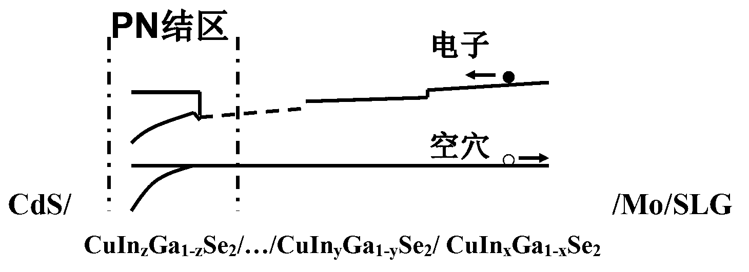
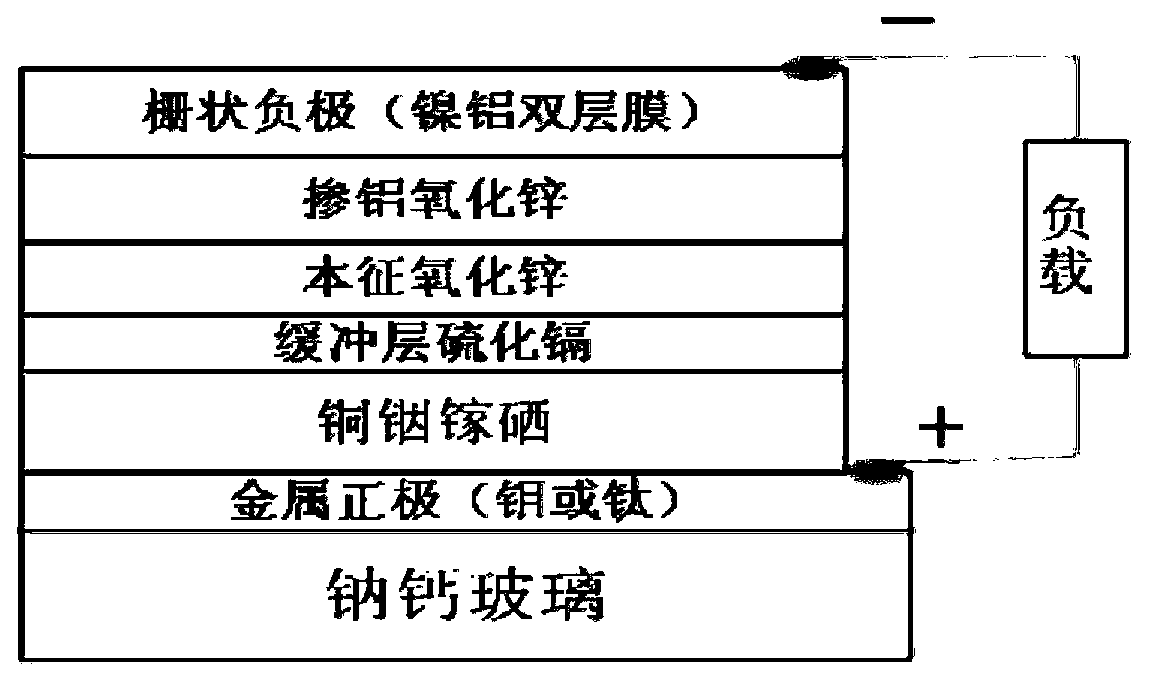
[0053] The substrate, metal positive electrode, light absorbing layer, buffer layer, window layer, transparent electrode layer and grid-shaped metal negative electrode are sequentially connected and assembled into a copper indium gallium selenide thin film solar cell;

[0054] Each copper indium gallium selenide monolayer of the light absorbing layer is directly formed into a film by adjusting the magnetron sputtering gas pressure, magnetron sputtering temperature range and magnetron sputtering power density, or preparing a prefabricated layer by magnetron sputtering, Then put the prefabricated layer under the protection of argon or nitrogen for 400~500 o C selenization treatment to form copper indium gallium selenide film; wherein the magnetron sputtering gas pressure is 0.1~10 Pa, and the magnetron sputtering temperature range is 200~600 o C, the ...

Embodiment 1

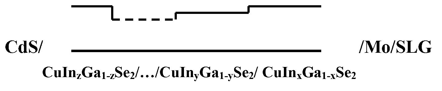
[0057] The copper indium gallium selenide thin film solar cell prepared in this embodiment includes a light absorption layer, which is arranged between the metal positive electrode and the buffer layer, and the light absorption layer is composed of two layers of copper indium gallium selenide with different energy gaps. The composition of the thin film, and the Ga composition in the CIGS single layer adjacent to the buffer layer is greater than the Ga composition in the remaining CIGS single layers.

[0058] The Ga composition refers to the atomic ratio of Ga / (In+Ga) in the CIGS thin film.

[0059] The atomic ratio of Ga / (In+Ga) in the single layer of copper indium gallium selenide adjacent to the metal positive electrode is 0.233, and its thickness is 300 nm; the atomic ratio of Ga / (In+Ga) in the second single layer of copper indium gallium selenide The ratio is 0.294, and its thickness is 300 nm;

[0060]The copper indium gallium selenide thin film solar cell of this embodi...

Embodiment 2

[0063] The copper indium gallium selenide thin film solar cell of this embodiment includes a light absorption layer, the light absorption layer is arranged between the metal positive electrode and the buffer layer, and the light absorption layer is composed of three layers of copper indium gallium selenide thin films with different energy gaps , the Ga composition in each CIGS monolayer is fixed, and the Ga composition in the CIGS monolayer adjacent to the buffer layer is greater than the Ga composition in the remaining CIGS monolayers.

[0064] The atomic ratio of Ga / (In+Ga) in the single layer of copper indium gallium selenide adjacent to the metal positive electrode is 0.302, and its thickness is 300 nm; the atomic ratio of Ga / (In+Ga) in the second single layer of copper indium gallium selenide ratio is 0.295, and its thickness is 300 nm; the atomic ratio of Ga / (In+Ga) in the third CIGS monolayer (the CIGS monolayer adjacent to the buffer layer) is 0.325, and its thickness i...


PUM

PropertyMeasurementUnit
thicknessaaaaaaaaaa
thicknessaaaaaaaaaa
thicknessaaaaaaaaaa

Abstract

The invention discloses a CIGS (copper indium gallium selenium) thin film solar cell and a preparation method thereof, and belongs to the technical field of the solar cell. The solar cell is formed by successively connecting a substrate, a metal anode, a light absorption layer, a buffer layer, a window layer, a transparent electrode layer and a grid-shaped metal cathode, wherein the light absorption layer consists of at least two layers of CIGS thin films of different energy gaps; and each CIGS single layer of the light adsorption layer is directly formed into the film by regulating the magnetron sputtering pressure, the temperature range and the power density, or a prefabricated layer is prepared by magnetron sputtering; and then, the prefabricated layer is subjected to selenylation processing to obtain the CIGS thin film at the temperature of 400-500DEG C under the protection of argon or nitrogen. Each single layer of CIGS thin film disclosed by the invention has different energy gaps, the shape of the energy band of the light absorption layer can be regulated in a combined mode, the collection and light spectrum response curve of a carrier can be both considered, and the absorption efficiency of the light absorption layer is improved by 30-50%. The CIGS thin film solar cell and the preparation method disclosed by the invention have the advantages of high cell photoelectric conversion efficiency, simple technology, simple required equipment and easiness in realizing mass production.

Description

technical field [0001] The invention belongs to the technical field of solar cells, and relates to the preparation of copper indium gallium selenium thin film solar cells and the structural design of thin film devices, in particular to a copper indium gallium selenium thin film solar cell and a preparation method thereof. Background technique [0002] Copper-indium-selenium-based thin-film solar cells are the new type of thin-film solar cells with the most market prospects because of their outstanding features such as high efficiency, low cost, long life, and flexible substrates. Copper indium selenide (CIS) has a chalcopyrite structure with an energy gap of 1.04 eV. If part of In in CIS is replaced by Ga, CuIn 1-x Ga x Se 2 The energy gap can be continuously adjusted between 1.04 and 1.68 eV, which provides an important theoretical basis for the preparation of copper indium gallium selenium thin film solar cells with adjustable energy gap. At present, the structure of co...

Claims


Application Information

Patent Timeline
Patent Type & Authority Applications(China)
IPC IPC(8): H01L31/032H01L31/0749H01L31/18
CPCY02E10/50Y02E10/541Y02P70/50
Inventor 王学进王胜利王文忠王志段东平
Owner CHINA AGRI UNIV
Why Eureka
Try Eureka