Avalanche photodetector and method for increasing high frequency characteristics of avalanche photodetector

An avalanche photoelectric, high-frequency characteristic technology, applied in the direction of circuits, electrical components, semiconductor devices, etc., can solve the problems of reduced capacitance of unfavorable devices, shortened carrier transit time, limited high-frequency performance of devices, etc., to achieve high-frequency The effect of improving the characteristics

Inactive Publication Date: 2013-05-01
INST OF SEMICONDUCTORS - CHINESE ACAD OF SCI
View PDF3 Cites 14 Cited by
  • Summary
  • Abstract
  • Description
  • Claims
  • Application Information

AI Technical Summary

Problems solved by technology

It can be seen that it takes a longer time for holes to be collected than electrons, which is not conducive to the shortening of

Method used


Image

  • Avalanche photodetector and method for increasing high frequency characteristics of avalanche photodetector
  • Avalanche photodetector and method for increasing high frequency characteristics of avalanche photodetector
  • Avalanche photodetector and method for increasing high frequency characteristics of avalanche photodetector

Examples


Embodiment Construction

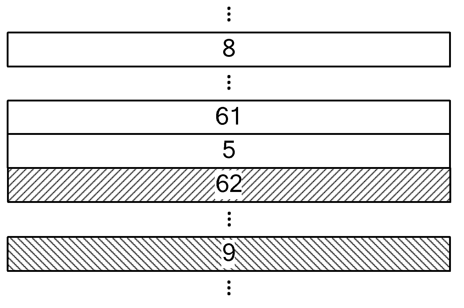
[0024] In order to more conveniently adjust the carrier transit time and the device capacitance of the avalanche photodetector (APD) and improve the high-frequency characteristics of the device, according to an aspect of the present invention, the APD in its longitudinal direction includes the original absorption layer, charge In addition to the layer and the multiplication layer, a transition layer is added, and the transition layer and the absorption layer are respectively located on both sides of the multiplication layer.

[0025] When the multiplication layer generates a large number of avalanche carrier pairs (electron-hole pairs) due to the avalanche effect, one type of carriers (such as holes) drifts longitudinally through the absorption layer to one end of the APD (from the multiplication layer the side with the absorber layer), another type of carriers (such as electrons) drift longitudinally through the transition layer (from the side with the transition layer of the ...


PUM


Abstract

The invention discloses an avalanche photodetector and a method for increasing high frequency characteristics of the avalanche photodetector. The avalanche photodetector is used for detecting target detecting light and comprises an absorbing layer (8), a first charge layer (61), a multiplication layer (5), a second charge layer (62) and a transition layer which are arrayed in turn along the longitudinal direction, wherein the absorbing layer (8) is used for absorbing the target detecting light and converting photons of the target detecting light into photo-produced free carrier pairs; the first charge layer (61) is used for regulating and controlling the electric field distribution in a device; the multiplication layer (5) is used for causing the free carriers entering into the multiplication layer to trigger an avalanche effect and generate avalanche carrier pairs; and one type of carrier in the avalanche carrier pairs longitudinally drifts to one end of the avalanche photodetector through the transition layer (9). The avalanche photodetector can better regulate the capacitance of the avalanche photodetector and the transition time of the carriers and is beneficial to the increasing of the high frequency characteristics of the avalanche photodetector.

Description

technical field [0001] The invention belongs to the field of semiconductor devices, in particular to an avalanche photodetector (APD) and a method for improving the high-frequency characteristics of the avalanche photodetector. Background technique [0002] Over the past five decades, avalanche photodetectors (APDs) have been widely used in commercial, military and scientific research, such as quantum information, biomolecular detection, lidar imaging, astronomical detection, etc. In recent years, the driving force of APD research mainly comes from optical communication. A high-speed, high-sensitivity APD with an operating wavelength of 1.55 μm is a key device for high-bit-rate long-distance optical fiber communications. Due to its intrinsic gain, APDs can be 5-10 dB more sensitive than PIN-type detectors. Over the past decade, the performance of APDs has significantly improved due to advances in materials and device structures. At present, APD has been successfully used ...

Claims


Application Information

Patent Timeline
IPC IPC(8): H01L31/107
Inventor 李彬韩勤杨晓红
Owner INST OF SEMICONDUCTORS - CHINESE ACAD OF SCI
Why Eureka
Try Eureka