N/n+ silicon epitaxial wafer with high metal impurity absorption capacity and preparation method thereof

A silicon epitaxial wafer, high-metal technology, applied in semiconductor/solid-state device manufacturing, electrical components, circuits, etc., can solve problems such as the inability to meet metal gettering, and achieve the goal of promoting metal gettering efficiency, excellent quality, and reducing power consumption. Effect

Active Publication Date: 2013-05-08
ZHEJIANG UNIV
View PDF5 Cites 1 Cited by
  • Summary
  • Abstract
  • Description
  • Claims
  • Application Information

AI Technical Summary

Problems solved by technology

However, when the donor doping concentration exceeds 10 19 / cm 3 At this time, according to the traditional ramping process and low-temperature-high-temperature heat treatment process in the past, the oxygen precipitation density obtained in the epitaxial wafer substrate is only 10 6 / cm 3 Or below, such a low density of oxygen precipitation cannot meet the needs of sufficient metal gettering

Method used


Image

  • N/n+ silicon epitaxial wafer with high metal impurity absorption capacity and preparation method thereof
  • N/n+ silicon epitaxial wafer with high metal impurity absorption capacity and preparation method thereof
  • N/n+ silicon epitaxial wafer with high metal impurity absorption capacity and preparation method thereof

Examples


Embodiment 1

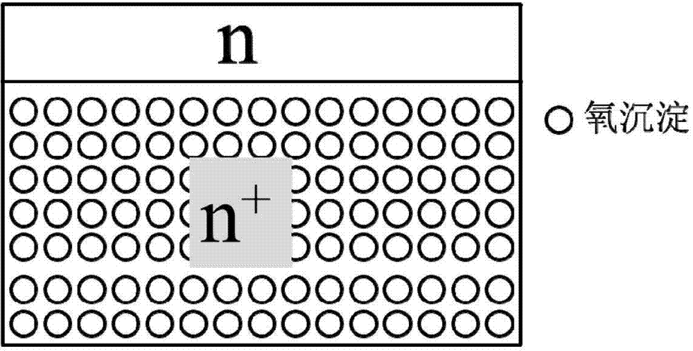
[0056] Production of n / n with high metal gettering ability based on heavily arsenic-doped Czochralski silicon + A method for preparing a silicon epitaxial wafer, comprising the following steps:

[0057] 1) Select heavily arsenic-doped Czochralski silicon with a diameter of 200mm in the crystal direction as n / n + The substrate of the silicon epitaxial wafer, the substrate resistivity is 0.003~0.005Ω·cm, and the oxygen concentration is 1.02×10 18 / cm 3 ;

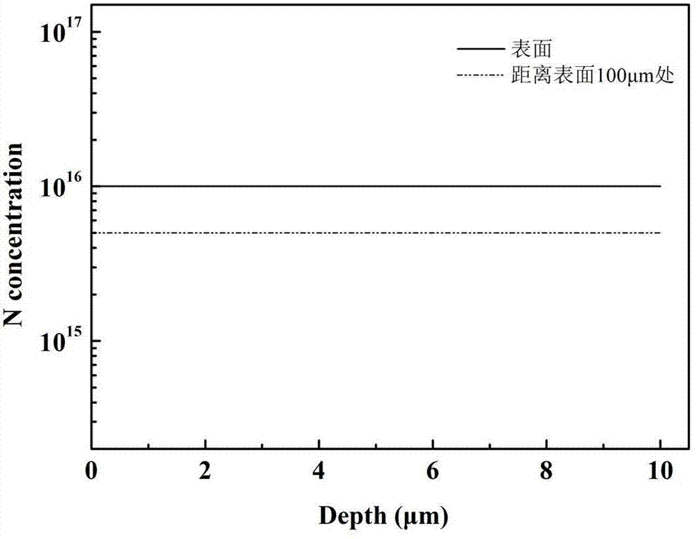
[0058] 2) After the heavily arsenic-doped Czochralski silicon was cleaned by RCA, it was placed in high-purity N 2 Heat treatment at 1260°C for 60s in a rapid heat treatment furnace under atmosphere, and rapidly cool at a cooling rate of 50°C / s to obtain a nitrogen-doped heavily arsenic-doped Czochralski silicon substrate;

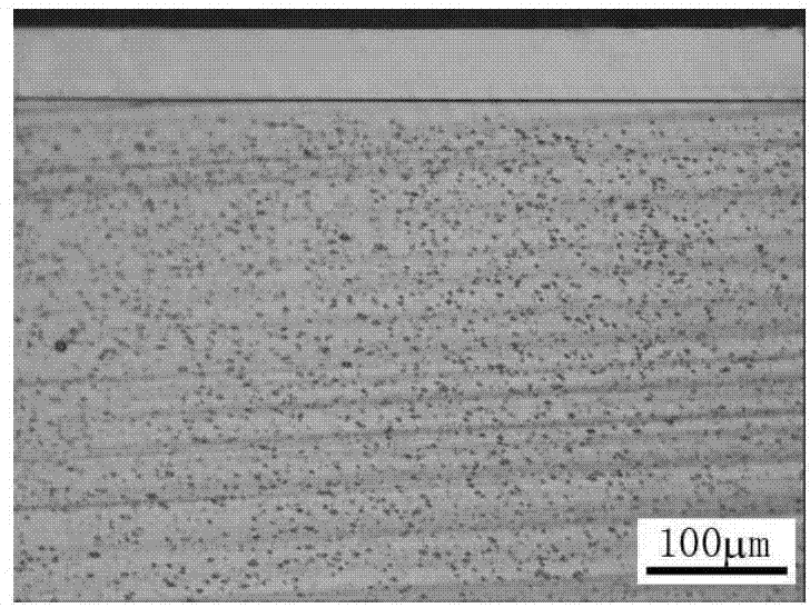
[0059] 3) Place the nitrogen-doped heavily arsenic-doped Czochralski silicon substrate in an epitaxy furnace, and grow a lightly phosphorous-doped silicon epitaxial layer with a thickness of 60 μm and...

Embodiment 2

[0102] Production of n / n with high metal gettering ability based on heavy antimony doped Czochralski silicon + A method for preparing a silicon epitaxial wafer, comprising the following steps:

[0103] 1) Select heavily antimony-doped Czochralski silicon with a diameter of 200mm in the crystal orientation as n / n + The substrate of the silicon epitaxial wafer, the substrate resistivity is 0.001~0.003Ω·cm, and the oxygen concentration is 7×10 17 / cm 3 ;

[0104] 2) After the heavily arsenic-doped Czochralski silicon was cleaned by RCA, it was placed in high-purity N 2 Heat treatment at 1200°C for 40s in a rapid heat treatment furnace under atmosphere, and rapidly cool at a cooling rate of 100°C / s to obtain a nitrogen-doped heavily antimony-doped Czochralski silicon substrate;

[0105] 3) Place the nitrogen-doped heavily antimony-doped Czochralski silicon substrate in an epitaxial furnace, and grow a lightly phosphorus-doped silicon epitaxial layer with a thickness of 20 μm ...

Embodiment 3

[0115] Production of n / n with high metal gettering ability based on heavily phosphorus-doped Czochralski silicon + A method for preparing a silicon epitaxial wafer, comprising the following steps:

[0116] 1) Choose heavily phosphorus-doped Czochralski silicon with a diameter of 200mm in the crystal orientation as n / n + The substrate of the silicon epitaxial wafer, the substrate resistivity is 0.002~0.004Ω·cm, and the oxygen concentration is 1.5×10 18 / cm 3 ;

[0117] 2) After the heavily arsenic-doped Czochralski silicon was cleaned by RCA, it was placed in high-purity N 2 Heat treatment at 1100°C for 200s in a rapid heat treatment furnace under atmosphere, and rapidly cool at a cooling rate of 40°C / s to obtain a nitrogen-doped heavily phosphorus-doped Czochralski silicon substrate;

[0118] 3) Place the nitrogen-doped heavily phosphorus-doped Czochralski silicon substrate in an epitaxial furnace, and grow a lightly phosphorus-doped silicon epitaxial layer with a thickne...


PUM

PropertyMeasurementUnit
electrical resistivityaaaaaaaaaa

Abstract

The invention provides a n/n+ silicon epitaxial wafer with a high metal impurity absorption capacity, and the n/n+ silicon epitaxial wafer with the high metal impurity absorption capacity includes that a light-doped n-type silicon is an epitaxial layer, defect density of the stacking fault and dislocation is less than or equal to 0.05 /cm2, nitrogen-doped heavy-doped n-type czochralski silicon is a substrate, and the resistivity of the substrate is less than or equal to 0.005 omega cm; the substrate contains a stable oxygen precipitation nucleation center, and the generated density of oxygen precipitation is more than or equal to 1 * 109 / cm3. The invention further provides a preparation method of the n/n+ silicon epitaxial wafer, and the steps of the preparation method include that the heavy-doped n-type czochralski silicon is carried out a high temperature rapid heat treatment under N2 atmosphere, and the light-doped n-type silicon epitaxial layer grows on the heat-treated heavy-doped n-type czochralski silicon. The n/n + silicon epitaxial wafer is acquired through two steps of heat treatment including a low temperature heat treatment and a high temperature heat treatment. The n/n+ silicon epitaxial wafer with a high metal impurity absorption capacity and the preparation method of the n/n+ silicon epitaxial wafer solve the problem that an oxygen precipitation with a high density is hard to generate in the n/n + silicon epitaxial wafer heavy-doped n-type czochralski silicon substrate, and have a good application prospect.

Description

technical field [0001] The invention belongs to the technical field of semiconductors, in particular to a n / n semiconductor with high metal gettering ability + Silicon epitaxial wafer and its preparation method. Background technique [0002] With heavily doped n-type Czochralski silicon as the substrate, lightly doped n-type silicon as the n / n of the epitaxial layer + Silicon epitaxial wafers are widely used in power devices, including MOS and bipolar devices, because they can significantly reduce the power consumption of power devices. [0003] In addition, another main feature of silicon epitaxial wafers is its superior metal gettering performance. Two gettering mechanisms, segregation gettering and internal gettering, determine the gettering efficiency of silicon epitaxial wafers. for n / n + For epitaxial wafers, the effective segregation and gettering requires that the doping concentration of the donor in the substrate is much higher than that in the epitaxial layer, ...

Claims


Application Information

Patent Timeline
Patent Type & Authority Applications(China)
IPC IPC(8): H01L29/06H01L21/18
Inventor 马向阳董鹏杨德仁
Owner ZHEJIANG UNIV
Why Eureka
Try Eureka