Thin film transistor array substrate, preparing method and display device

A technology of thin film transistors and array substrates, applied in the field of display, can solve the problems of low production efficiency, high production cost, waste of materials for forming pixel electrodes, etc., and achieve the effects of improving utilization rate, reducing usage, and reducing production cost

Active Publication Date: 2013-06-12
BOE TECH GRP CO LTD
View PDF5 Cites 21 Cited by
  • Summary
  • Abstract
  • Description
  • Claims
  • Application Information

AI Technical Summary

Problems solved by technology

In the preparation process of thin film transistors, in order to form the pattern of the pixel electrode layer, it is necessary to form a certain thickness of indium tin oxide film layer by sputtering, and then transfer the pattern to the indium tin oxide film layer by means of photolithography processes such as mask exposure. on, resulting in the waste of pixel electrode forming materials
At the same time, in the preparation process of the thin film transistor array substrate, the more masks are used, the lower the production efficiency and the higher the production cost.

Method used


Image

  • Thin film transistor array substrate, preparing method and display device
  • Thin film transistor array substrate, preparing method and display device
  • Thin film transistor array substrate, preparing method and display device

Examples


preparation example Construction

[0027] A method for preparing a thin film transistor array substrate, comprising the following steps: forming a gate electrode layer, a gate insulating layer, an active layer, a source-drain electrode layer, and a passivation layer on the substrate, wherein the passivation layer is formed by a patterning process The structural pattern includes a via hole, the pixel electrode layer is formed in the structural pattern area by dripping, and the source and drain electrode layers are connected to the pixel electrode layer through the via hole.

[0028] A thin film transistor array substrate is formed by the above method for preparing a thin film transistor array substrate.

[0029] A display device includes the above thin film transistor array substrate.

Embodiment 1

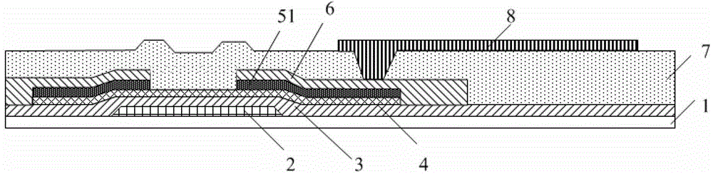
[0031] like image 3 As shown, the thin film transistor array substrate in this embodiment includes forming a gate electrode layer 2, a gate insulating layer 3, an active layer 4, a source-drain electrode layer 6, and a passivation layer 7 on a substrate 1 (also called a substrate). and the pixel electrode layer 8 . Wherein, the passivation layer 7 forms a structural pattern including via holes through a patterning process, the pixel electrode layer 8 is formed in the structural pattern area by dripping, and the source and drain electrode layers 6 and the pixel electrode layer 8 Connect via vias.

[0032] In this embodiment, the active layer 4 is formed of amorphous silicon material, correspondingly, an ohmic contact layer 51 is formed on the active layer 4, and the ohmic contact layer 51 is made of doped phosphorus element Formed from amorphous silicon material, the typical cross-sectional view of the thin film transistor array substrate is as follows image 3 shown.

[0...

Embodiment 2

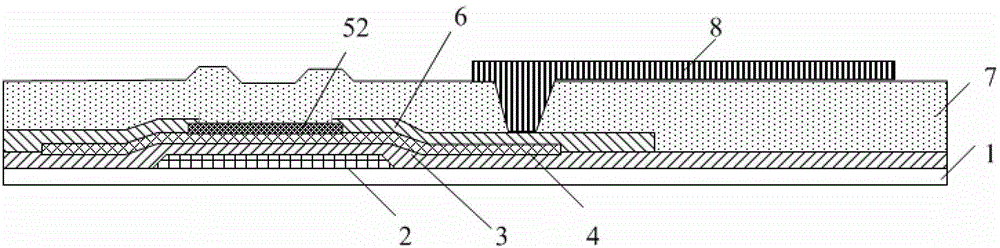
[0053] The difference between this embodiment and Embodiment 1 is that the active layer 4 in the thin film transistor array substrate of this embodiment is formed of a metal oxide semiconductor. A typical cross-sectional view of the thin film transistor array substrate is as follows Figure 5 shown.

[0054] In this embodiment, the preparation process of the thin film transistor array substrate is as follows: Figures 6a-6g shown.

[0055] Among them, such as Figure 6c As shown, an active layer 4 is formed on the gate insulating layer 3 . In this embodiment, the active layer 4 is formed of a metal oxide semiconductor made of oxygen (O) and indium (In), gallium (Ga), zinc (Zn), tin At least two elements in (Sn) are formed (that is, it must contain oxygen), and the active layer uses indium gallium zinc oxide (IGZO), indium zinc oxide (IZO), indium tin oxide (InSnO), indium gallium oxide Tin (InGaSnO) forms, preferably IGZO and IZO. The active layer is formed by sputtering,...


PUM


Abstract

The invention relates to a preparing method of a thin film transistor array substrate, a thin film transistor array substrate and a display device, and belongs to the displaying technical field. The preparing method comprises the following steps of: forming a gate electrode layer, a gate insulation layer, an active layer, a source and drain electrode layer, a passivation layer and a pixel electroed layer on the substrate, wherein the passivation layer forms a structure pattern comprising through holes through a composition technology, the pixel electrode layer is formed in the structure pattern region by a dripping mode, and the source and drain electrode layer is connected with the pixel electrode layer through the through holes. By the preparing method, the steps for forming the pixel electrode layer by the composition technology are reduced, the usage amount of a mask plate is reduced, the use ratio of the pixel electrode forming material is improved, and the production cost is reduced.

Description

technical field [0001] The invention belongs to the field of display technology, and in particular relates to a preparation method of a thin film transistor array substrate, a thin film transistor array substrate and a display device. Background technique [0002] In recent years, display technology has developed rapidly, such as thin film transistor (ThinFilmTransistor: TFT for short) technology has developed from the original amorphous silicon thin film transistor to the current low temperature polysilicon thin film transistor, metal oxide semiconductor thin film transistor and so on. The light-emitting technology has also developed from the original Liquid Crystal Display (LCD for short) technology to the current Organic Light-Emitting Diode (OLED for short) technology. [0003] As a driving element of a display device, a thin film transistor is directly related to the development direction of a high-performance flat panel display device. A thin film transistor generally...

Claims


Application Information

Patent Timeline
Patent Type & Authority Applications(China)
IPC IPC(8): H01L21/77H01L27/12
CPCH01L29/66765H01L27/1225H01L27/1292G02F1/136227G02F1/136236G02F1/136231H10K59/123H10K59/124H10K50/81
Inventor 孔祥永刘晓娣成军陈江博
Owner BOE TECH GRP CO LTD
Why Eureka
Try Eureka