Organic thin film transistor, preparation method and preparation device thereof

A technology of organic thin film and preparation device, which is applied in the direction of surface coating liquid device, semiconductor/solid-state device manufacturing, electric solid-state device, etc. It can solve the problems of uniformity difference, waste of raw materials, and difficulty in applying flexible substrates, etc. Achieve the effect of improving yield and good performance uniformity

Inactive Publication Date: 2013-06-12
BOE TECH GRP CO LTD
View PDF5 Cites 19 Cited by
  • Summary
  • Abstract
  • Description
  • Claims
  • Application Information

AI Technical Summary

Problems solved by technology

Another point, the spin coating method will throw off most of the solution, resulting in waste of raw materials
In addition, the spin-coating method is also difficult to apply to flexible substrates
Based on the above factors, this preparation method is difficult to achieve industrial application
[0007] The defect of the prior art is that, using the spin-coating process, the difference between the linear speed at the center of the substrate and the linear speed at the edge of the substrate leads to a large drop between the center and the edge, and poor uniformity, which makes the crystallization direction of the semiconductor material chaotic, resulting in device low yield

Method used


Image

  • Organic thin film transistor, preparation method and preparation device thereof
  • Organic thin film transistor, preparation method and preparation device thereof
  • Organic thin film transistor, preparation method and preparation device thereof

Examples


preparation example Construction

[0058] The preparation method of the organic thin film transistor of the present invention comprises:

[0059] Forming a gate electrode, a gate insulating layer, an organic semiconductor layer and source and drain electrodes on the substrate;

[0060] Wherein, the step of forming the organic semiconductor layer comprises:

[0061] The solution in which the organic semiconductor material used to form the organic semiconductor layer is dissolved is blade-coated to form the organic semiconductor layer.

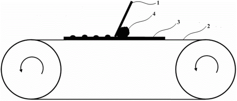
[0062] In the technical solution of the present invention, the prepared solution is scraped and coated on the substrate through a scraping process, and the scraper can be scraped on the substrate by moving along a straight line, or by rotating the scraper on the substrate. , during the entire scraping process, the scraper makes the transverse shear force of the solution on the substrate consistent, the thickness of the solution is consistent, and the state of each device is equa...

Embodiment 1

[0111] Dissolve Tips-pentacene and polystyrene (PS) with a mass ratio of 1:1 in chlorobenzene at 40°C, let it stand and filter to prepare the total mass of Tips-pentacene and polystyrene Divide a mixed solution with a concentration of 2%, titrate a sufficient amount of the solution on the edge of the silicon substrate, and slowly and evenly scrape the solution on the silicon substrate at a speed of 0.5mm / s to complete the selective patterning, and dry it overnight in a vacuum environment. Prepare the film. A metal baffle covers the self-assembled device, and a gold electrode with a thickness of 50-100 nm is prepared as a source-drain electrode by thermal evaporation.

Embodiment 2

[0113] Dissolve Tips-pentacene and polystyrene (PS) with a mass ratio of 1:1 in chlorobenzene at 40°C, let it stand and filter to obtain the total mass percentage of Tips-pentacene and polystyrene An organic solution with a concentration of 2%, titrate a sufficient amount of the solution on the edge of the silicon substrate, and slowly and evenly coat the solution on the silicon substrate at a speed of 5cm / s by means of an additional scraping device to complete the selective patterning, vacuum The environment was dried overnight to prepare a film. A metal baffle covers the self-assembled device, and a gold electrode with a thickness of 50-100 nm is prepared as a source-drain electrode by thermal evaporation.


PUM


Abstract

The invention relates to the field of liquid crystal display and discloses an organic thin film transistor, a preparation method and a preparation device thereof. The preparation method for the organic thin film transistor comprises the steps that a grid electrode, a grid insulation layer, an organic semiconductor layer, a source electrode and a drain electrode are formed on a substrate; the organic semiconductor layer forming procedures include that a solution in which an organic semiconductor material used for forming the organic semiconductor layer is dissolved is subjected to blade coating, so that the organic semiconductor layer is formed. By adopting the technical scheme of the invention, in the blade coating process, the transverse shearing force applied on the solution in each row or column of the substrate is consistent, the thickness of the solution formed through the blade coating is consistent, the state of each device is equal, the difference between the edge and the center of the substrate, caused by centripetal force with the adoption of the rotary coating technique is avoided, and the defect-free rate of the organic thin film transistor devices is improved.

Description

technical field [0001] The invention relates to the technical field of liquid crystal display, in particular to an organic thin film transistor, a preparation method thereof, and a preparation device. Background technique [0002] Organic Thin Film Transistor (OTFT for short) is a semiconductor device that uses organic materials instead of traditional silicon semiconductor materials. Compared with silicon-based materials, organic materials are difficult to process and cost high. However, organic materials can be prepared into solutions and semiconductor devices can be prepared under mild conditions. Therefore, they have attracted more attention and have become the core link in the next generation of display technology. At present, many display giants such as Samsung and Sony have begun to develop integrated circuits based on organic thin film transistors. Organic thin film transistors have also become an indispensable technical component in foldable displays and panoramic d...

Claims


Application Information

Patent Timeline
Patent Type & Authority Applications(China)
IPC IPC(8): H01L51/40H01L51/10
CPCY02E10/549H10K71/12H10K85/623H10K85/40H10K10/466H10K77/10B05C1/00
Inventor 邱龙臻冯翔王向华刘则
Owner BOE TECH GRP CO LTD
Why Eureka
Try Eureka