Laser processing device and laser processing method

A technology of laser processing device and laser light source, which is applied in laser welding equipment, electrical components, circuits, etc.

Active Publication Date: 2013-06-12
JSW阿克迪纳系统有限公司
View PDF8 Cites 17 Cited by
  • Summary
  • Abstract
  • Description
  • Claims
  • Application Information

AI Technical Summary

Problems solved by technology

[0005] In addition, Patent Document 2 describes that in a two-wavelength laser surface treatment device that uses a fundamental wave light pulse and a higher harmonic light pulse to irradiate a sample to be condensed, the fundamental wave light pulse or the higher harmonic light pulse Any one of the delays, so that at least a delay of more than the pulse duration of the optical pulse is generated between the two pulses

Method used


Image

  • Laser processing device and laser processing method
  • Laser processing device and laser processing method
  • Laser processing device and laser processing method

Examples


Embodiment 1

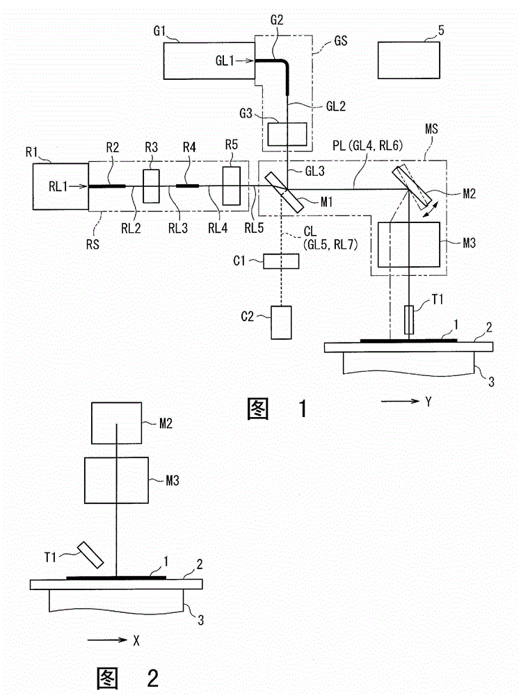
[0129] according to figure 1 , figure 2 A laser processing apparatus according to an embodiment of the present invention will be described.

[0130] The laser processing device of this embodiment includes: a visible laser light source G1 that outputs pulsed waves, that is, visible laser light GL1 , and a near-infrared laser light source R1 that outputs continuous waves, that is, near-infrared laser RL1 .

[0131] Visible laser light source G1 is, for example, a laser oscillator that performs pulse oscillation with an output power of 50W, a vibration frequency of 10kHz, and a pulse energy of 5mJ to generate green laser light with a wavelength of 532nm, which is a frequency doubled wave of YAG laser. In addition, the wavelength of the visible laser light of this invention is not limited to a specific value, For example, the wavelength of 355-577 nm can be illustrated.

[0132] In addition, the near-infrared laser light source R1 is, for example, a semiconductor laser that con...

Embodiment 2

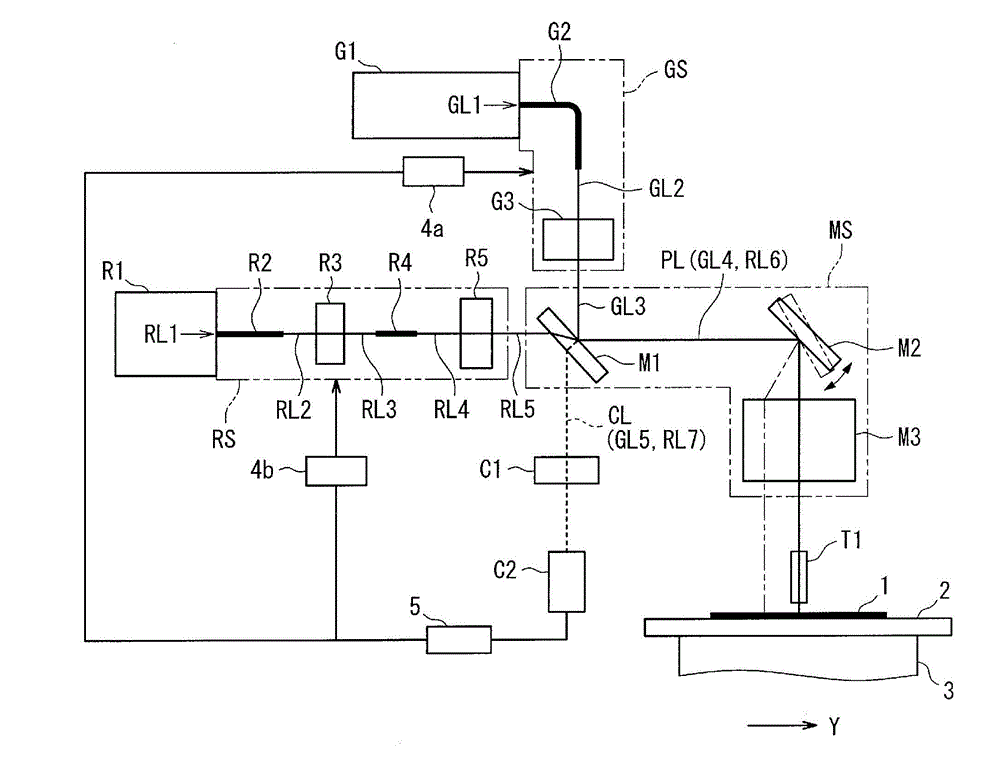
[0185] Next, according to Figure 4 A laser processing apparatus according to another embodiment of the present invention will be described. In addition, the same code|symbol is attached|subjected to the same structure as said Example 1, and the description is abbreviate|omitted or simplified.

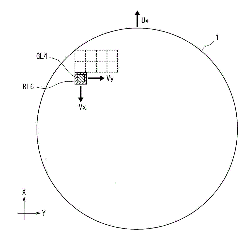
[0186] The irradiation positions of the visible laser GL4 and the near-infrared laser RL6 on the object 1 may not only be aligned with appropriate positions, but may also be offset from each other. If the irradiation positions of the two laser beams are shifted, there is a possibility that the processing cannot be performed properly. In this embodiment, there is provided a mechanism for adjusting the deviation of the irradiation positions of the visible laser light GL4 and the near-infrared laser light RL6.

[0187] In this embodiment, the optical fiber G2 and the collimator lens G3 constituting the visible light optical system GS are provided with an adjustment mechanism 4a for adju...

Embodiment 3

[0199] Next, according to Image 6 Another embodiment will be described. In addition, the same code|symbol is attached|subjected to the same structure as each said Example, and the description is simplified.

[0200] The laser processing device of this embodiment includes: a visible laser light source G1 outputting a pulse wave, that is, a visible laser GL10 , and a near-infrared laser light source R1 outputting a continuous wave, that is, a near-infrared laser RL10 .

[0201] In this embodiment, the visible laser light source G1 is, for example, pulsed with an output power of 50W, a vibration frequency of 10kHz, and a pulse energy of 5mJ to generate a green laser with a wavelength of 532nm and a pulse width of 100ns, which is a doubled wave of YAG laser. The wavelength of the visible laser light of the visible laser light source G1 is not limited to a specific wavelength, and examples thereof include wavelengths in the range of 355 to 577 nm.

[0202] Also, in this embodime...


PUM


Abstract

An objective of the present invention is to allow projecting a visible light laser beam and a near-infrared laser beam on a body to be processed such as a wafer with an inexpensive device configuration with a high degree of controllability, and to allow laser processing the body to be processed with a high degree of productivity. A laser beam processing device comprises: a visible light laser light source (G1) which outputs a visible light laser beam; a visible light optical assembly (GS (an optical fiber (G2) and a collimator lens (G3)) which wave guides the visible light laser beam; a near-infrared laser light source (R1) which outputs a near-infrared laser beam; a near-infrared optical assembly (RS (an optical fiber (R2), a light collection lens (R3), an optical fiber (R4), and a collimator lens (R5)) which wave guides the near-infrared laser beam; and a multiplexing optical assembly (MS (a dichroic mirror (M1), a galvano mirror (M2), and an f theta lens (M3)), which multiplexes the visible light laser beam, which is wave guided by the visible light optical assembly (GS) and the near-infrared laser beam which is wave guided by the near-infrared optical assembly (RS), and wave guides same to the body to be processed (1).

Description

technical field [0001] The present invention relates to a laser processing device and a laser processing method that irradiate a target object with laser light to perform predetermined processing. Background technique [0002] In the manufacturing process of a semiconductor device, a semiconductor wafer into which impurities have been introduced by ion implantation or the like is subjected to heat treatment for the purpose of activating the impurities and recovering crystal damage. As such a heat treatment method, in addition to furnace annealing in which a semiconductor wafer is heated in a heating furnace, laser annealing in which a semiconductor wafer is heated by irradiating laser light is known. [0003] As laser annealing, for example, a method of irradiating a substrate such as a semiconductor wafer with two laser beams having different wavelengths has been proposed (see Patent Document 1 and Patent Document 2). [0004] Patent Document 1 describes a semiconductor de...

Claims


Application Information

Patent Timeline
Patent Type & Authority Applications(China)
IPC IPC(8): H01L21/268B23K26/00B23K26/06B23K26/073B23K26/08H01L21/20H01L21/265
CPCB23K26/032B23K26/0732B23K26/082H01L21/02678H01L21/02691H01L21/268B23K26/08B23K26/064
Inventor 小林直之山口芳广清野俊明工藤利雄
Owner JSW阿克迪纳系统有限公司
Why Eureka
Try Eureka