Tellurium-cadmium-mercury grid-controlled structure photoconductive detector for Hall test

A mercury cadmium telluride and structured light technology, which is applied in the direction of semiconductor devices, sustainable manufacturing/processing, electrical components, etc., to achieve the effect of shortening the development process and simplifying the preparation process

Inactive Publication Date: 2013-06-19
SHANGHAI INST OF TECHNICAL PHYSICS - CHINESE ACAD OF SCI
View PDF2 Cites 8 Cited by
  • Summary
  • Abstract
  • Description
  • Claims
  • Application Information

AI Technical Summary

Problems solved by technology

[0004] At present, there is no public report on the HgCdTe gate-controlled photoconductive detector used for Hall testing. The use of this structure to prepare the HgCdTe gate-controlled detector overcomes the traditional gate-controlled device, which only measures the device under the condition of an external grid voltage. The shortcomings of detector performance parameters such as high responsivity and detectability, after the completion of the device preparation, not only the performance of the detector can be teste...

Method used


Image

  • Tellurium-cadmium-mercury grid-controlled structure photoconductive detector for Hall test

Examples


example 1

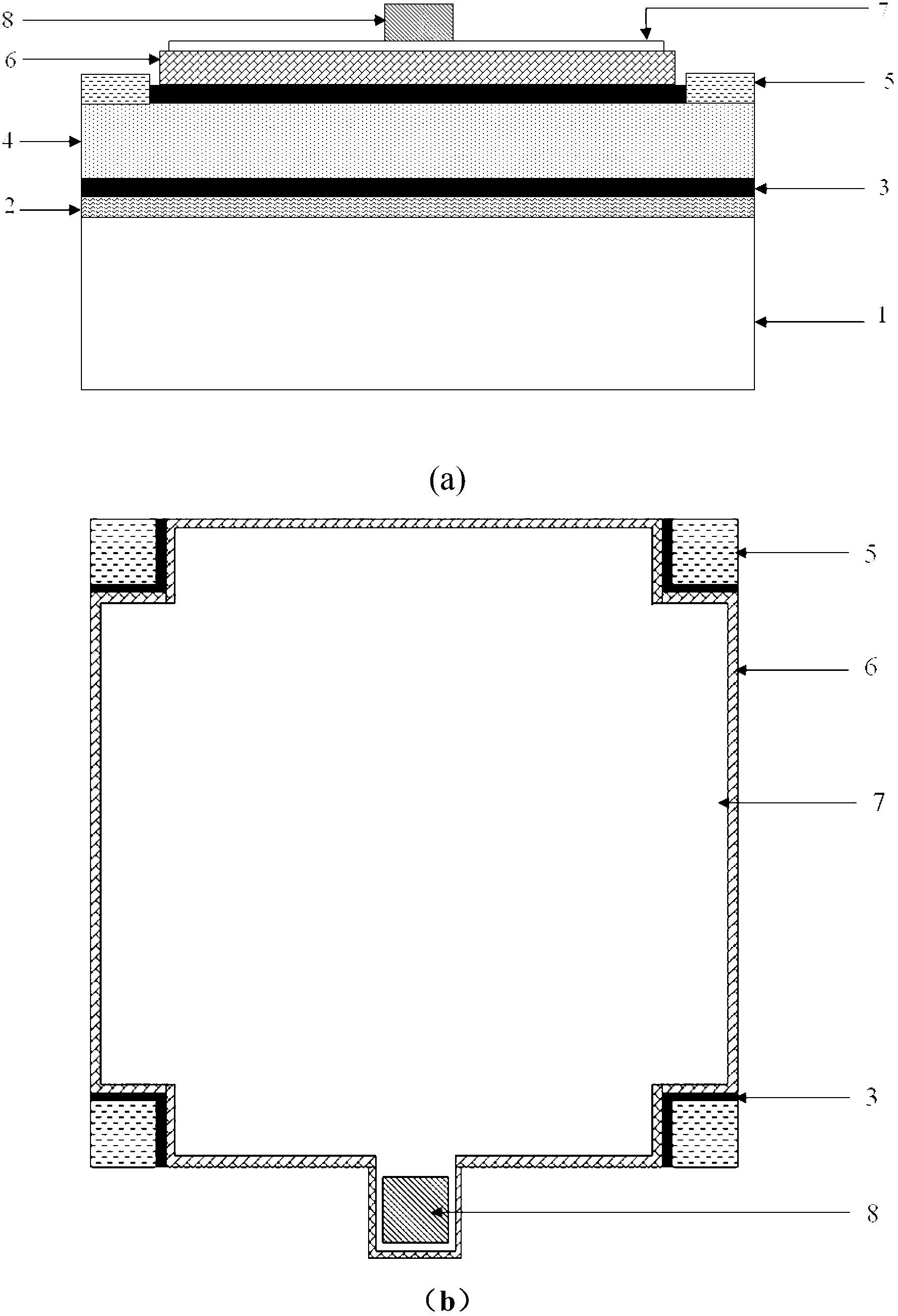
[0018] Step 1: De-damaging the flatness of the first surface of the n-type HgCdTe material 4, wherein Hg 1-x Cd x In Te, x=0.21, at liquid nitrogen temperature, the mobility is about 3×10 4 cm 2 / (V s), the electron concentration is about 1×10 13 cm -3 . An anodized layer 3 with a thickness of 80 nm is grown on its surface.

[0019] Step 2: Paste the processed side of the mercury cadmium telluride material 4 with the sapphire substrate 1 with the prepared epoxy resin glue 2, and fully cure under pressure at a certain temperature (about 60°C) under vacuum to ensure The adhesive layer is within a certain uniform thickness range, and the curing time is about 90mins to ensure the adhesive strength.

[0020] Step 3: Paste the processed chip on the first side on the ground glass plate with wax, and then flatten it with a vacuum silicon wafer machine (to ensure that the thickness difference is within 3 μm), and make the other side of the mercury cadmium telluride material In t...

example 2

[0030] Step 1: De-damaging the flatness of the first surface of the n-type HgCdTe material 4, wherein Hg 1-x Cd x In Te, x=0.26, at liquid nitrogen temperature, the mobility is about 1×10 5 cm 2 / (V·s), the electron concentration is about 2×10 14 cm -3 . An anodized layer 3 with a thickness of 90 nm is grown on its surface.

[0031] Step 2: Paste the processed side of the mercury cadmium telluride material 4 with the sapphire substrate 1 with the prepared epoxy resin glue 2, and fully cure under pressure at a certain temperature (about 60°C) under vacuum to ensure The adhesive layer is within a certain uniform thickness range, and the curing time is about 90mins to ensure the adhesive strength.

[0032] Step 3: Paste the processed chip on the first side on the ground glass plate with wax, and then flatten it with a vacuum silicon wafer machine (to ensure that the thickness difference is within 3 μm), and make the other side of the mercury cadmium telluride material Thin...

example 3

[0042] Step 1: De-damaging the flatness of the first surface of the n-type HgCdTe material 4, wherein Hg 1-x Cd x In Te, x=0.23, at liquid nitrogen temperature, the mobility is about 5×10 4 cm 2 / (V s), the electron concentration is about 1×10 15 cm -3 . An anodized layer 3 with a thickness of 100 nm is grown on its surface.

[0043] Step 2: Paste the processed side of the mercury cadmium telluride material 4 with the sapphire substrate 1 with the prepared epoxy resin glue 2, and fully cure under pressure at a certain temperature (about 60°C) under vacuum to ensure The adhesive layer is within a certain uniform thickness range, and the curing time is about 90mins to ensure the adhesive strength.

[0044] Step 3: Paste the processed chip on the first side on the ground glass plate with wax, and then flatten it with a vacuum silicon wafer machine (to ensure that the thickness difference is within 3 μm), and make the other side of the mercury cadmium telluride material Thi...


PUM

PropertyMeasurementUnit
Thicknessaaaaaaaaaa
Thicknessaaaaaaaaaa
Electron concentrationaaaaaaaaaa

Abstract

The invention discloses a tellurium-cadmium-mercury grid-controlled structure photoconductive detector for Hall test. The tellurium-cadmium-mercury grid-controlled structure photoconductive detector structurally comprises a substrate, a tellurium-cadmium-mercury material, epoxy resin glue, a ZnS passivation layer, four Hall electrodes, a transparent grid electrode and a thickened electrode, the substrate is a sapphire wafer, the tellurium-cadmium-mercury material grows an anodic oxide layer after double-faced rough polishing and fine polishing, the epoxy resin glue is used for bonding the tellurium-cadmium-mercury material and the substrate, the ZnS passivation layer can function in passivating the surface of the material and increasing permeability, the four Hall electrodes positioned in the front and the rear grow on the tellurium-cadmium-mercury material and serve as signal extraction electrodes for the Hall test and device performance test, the transparent grid electrode grows on the ZnS passivation layer and is used for applying grid voltage to a device, and the thickened electrode grows on the transparent grid electrode. The detector with the structure can apply the grid voltage in the device performance test process and the Hall test process to obtain needed electrical parameter conditions such as the grid voltage, material carrier concentration and mobility when device performances are optimal, and the development process of the device is greatly shortened.

Description

technical field [0001] The invention relates to infrared photoelectric detection technology, in particular to a mercury cadmium telluride grid-controlled photoconductive detector grown with a Hall electrode and a transparent grid electrode. Background technique [0002] With the advancement of infrared technology and the development of space remote sensing applications, the ternary compound semiconductor material HgCdTe can continuously adjust the band gap with the composition, and the response range covers the entire infrared band (including 1~3μm, 3~5μm And 8 ~ 14μm three atmospheric windows), has become the material of choice for the development of units, multi-element infrared detectors and infrared focal planes. [0003] Due to the narrow bandgap of HgCdTe materials, the devices prepared are significantly affected by surface and interface characteristics, especially for HgCdTe infrared detectors in the long-wave and very long-wave bands, and may even become the dominant...

Claims


Application Information

Patent Timeline
IPC IPC(8): H01L31/112H01L31/0224H01L31/18
CPCY02P70/50
Inventor 徐鹏霄张可锋李向阳刘新智赵水平朱龙源刘福浩张立瑶
Owner SHANGHAI INST OF TECHNICAL PHYSICS - CHINESE ACAD OF SCI
Why Eureka
Try Eureka