N-type injection infrared wavelength-to-visible wavelength upconversion device and manufacturing device thereof

A conversion device, N-type technology, applied in sustainable manufacturing/processing, climate sustainability, final product manufacturing, etc., can solve problems such as low light utilization efficiency, low conversion efficiency, and difficulty in injecting photogenerated holes, so as to promote The effect of high transmission and conversion efficiency and simple preparation process

Active Publication Date: 2013-06-19
INST OF SEMICONDUCTORS - CHINESE ACAD OF SCI
View PDF4 Cites 37 Cited by
  • Summary
  • Abstract
  • Description
  • Claims
  • Application Information

AI Technical Summary

Problems solved by technology

It can solve the problem of low conversion efficiency of existing organic-inorganic composite wavelength up-conversion devices due to difficulties in injecting photogenerated holes and low light utilization efficiency.

Method used


Image

  • N-type injection infrared wavelength-to-visible wavelength upconversion device and manufacturing device thereof
  • N-type injection infrared wavelength-to-visible wavelength upconversion device and manufacturing device thereof
  • N-type injection infrared wavelength-to-visible wavelength upconversion device and manufacturing device thereof

Examples


preparation example Construction

[0043] Figure 4 A flow chart of the preparation method of the N-type implanted infrared-to-visible wavelength up-conversion device proposed by the present invention is shown. Such as Figure 4 As shown, the present invention also proposes a specific preparation method of an N-type implanted infrared-to-visible wavelength up-conversion device, which includes the following steps:

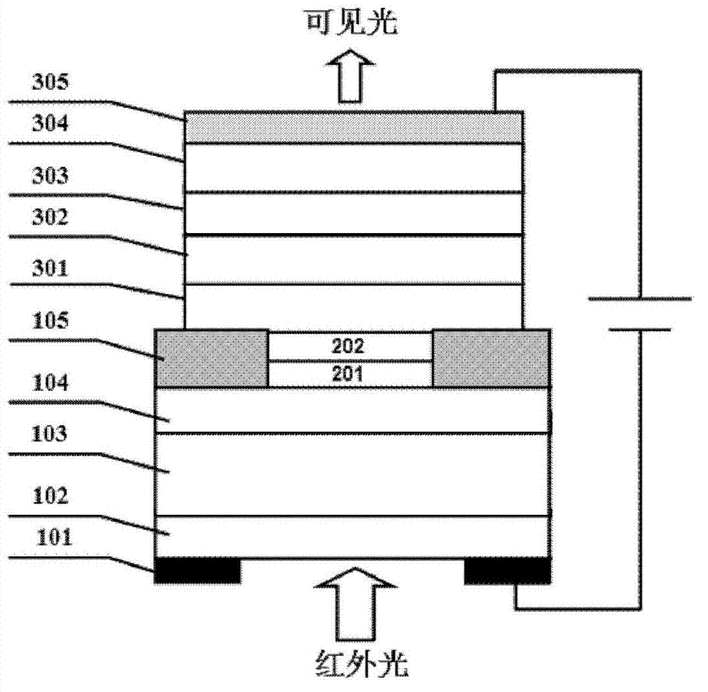
[0044] Step 1, using semiconductor thin film epitaxy techniques such as molecular beam epitaxy (MBE) or metal organic chemical vapor deposition (MOCVD) to grow the material structure of the infrared detector unit 103 on the substrate 102; then grow N-type on the infrared detector unit 103 spacer layer 104 .

[0045] Step 2, using semiconductor processing technology to prepare the device structure of the infrared detector unit 103;

[0046] Step 3, making the cathode layer 101 on the back side of the substrate 102;

[0047] Step 4, preparing an insulating window layer 105 on the top of the N-type ...

Embodiment 1

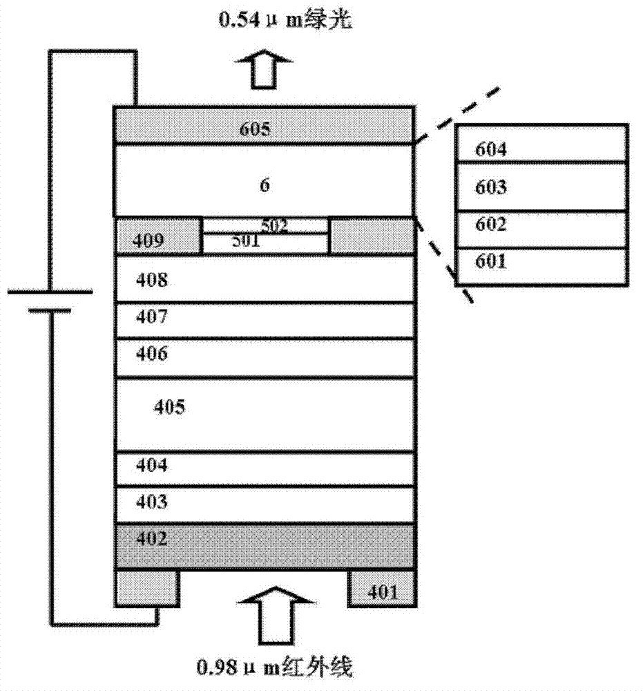
[0057] figure 2 It shows a schematic cross-sectional view of the N-type implanted infrared-to-visible wavelength up-conversion device in a preferred embodiment of the present invention, wherein the inorganic infrared detector unit is based on a GaAs / InGaAs multiple quantum well structure. The N-type implanted infrared-to-visible wavelength up-conversion imaging device can realize up-conversion of wavelengths from 0.98 μm to 0.54 μm, and its preparation method is as follows:

[0058] Step 1. Using a molecular beam epitaxy system to epitaxially grow an infrared detector unit on a P-type GaAs substrate 402, the details are as follows:

[0059] 1) Epitaxially grow a P-type GaAs buffer layer 403 on a P-type GaAs substrate 402 with a thickness of 200 nm and a P-type doping concentration of 3×10 18 cm -3 ;

[0060] 2) epitaxially growing an intrinsic GaAs layer 404 on the P-type GaAs buffer layer 403 with a thickness of 5 nm;

[0061] 3) Epitaxial growth of 60 cycles of GaAs / In ...


PUM


Abstract

The invention discloses an N-type injection infrared wavelength-to-visible wavelength upconversion device and a manufacturing device thereof. An inverted organic light emitting diode (OLED) is epitaxially grown on an inorganic infrared detector on the lower part. According to a work principle of the device, the infrared detector unit which is reversely biased converts the input infrared signal to an electrical signal, and photoinduced electrons sequentially flow through an N-type spacing layer and a light limiting metal layer and are injected into the OLED which is biased forward, and the OLED is driven to emit visible light, so that the infrared light-to-visible light upconversion can be realized. The provided N-type injection infrared wavelength-to-visible wavelength upconversion device has the characteristics of high conversion efficiency, wide conversion wavelength range, simple manufacturing process, low cost and the like and can be used for fields of infrared night vision, medical detection, industrial fault detection and the like.

Description

technical field [0001] The invention relates to the technical field of infrared detectors, organic electroluminescent diodes and semiconductors, in particular to an N-type implanted infrared-to-visible wavelength upconversion device composed of an inorganic infrared detector and an inverted organic electroluminescent diode coupled in series and its preparation method. Background technique [0002] Infrared imaging technology has a very wide range of practical value in civilian night vision, industrial flaw detection, wafer inspection, medical inspection, atmospheric imaging, military reconnaissance and other fields. At present, the traditional infrared imager uses the infrared focal plane detection array to convert the infrared light signal into an electrical signal, and then amplifies it through the interconnected readout circuit, and converts it into a video signal that can be used by the display screen. However, the method of connecting the detection part and the display...

Claims


Application Information

Patent Timeline
Patent Type & Authority Applications(China)
IPC IPC(8): H01L31/147H01L31/18
CPCY02P70/50
Inventor 楚新波关敏曾一平王宝强朱战平
Owner INST OF SEMICONDUCTORS - CHINESE ACAD OF SCI
Why Eureka
Try Eureka