Complementary metal oxide semiconductor (CMOS) amplifying circuit matched with infrared low-impedance photoconductive detector

A technology of amplifying circuit and low impedance, which is applied in the field of CMOS circuit design to reduce system noise and ensure bandwidth

Inactive Publication Date: 2013-06-19
SHANGHAI INST OF TECHNICAL PHYSICS - CHINESE ACAD OF SCI
View PDF1 Cites 1 Cited by
  • Summary
  • Abstract
  • Description
  • Claims
  • Application Information

AI Technical Summary

Problems solved by technology

[0003] The purpose of the present invention is to overcome the deficiencies of the existing conditions, a CMOS circuit is designed, the bridge input mode is adopted in the front end, and the problem of m...

Method used


Image

  • Complementary metal oxide semiconductor (CMOS) amplifying circuit matched with infrared low-impedance photoconductive detector
  • Complementary metal oxide semiconductor (CMOS) amplifying circuit matched with infrared low-impedance photoconductive detector
  • Complementary metal oxide semiconductor (CMOS) amplifying circuit matched with infrared low-impedance photoconductive detector

Examples


Embodiment 1

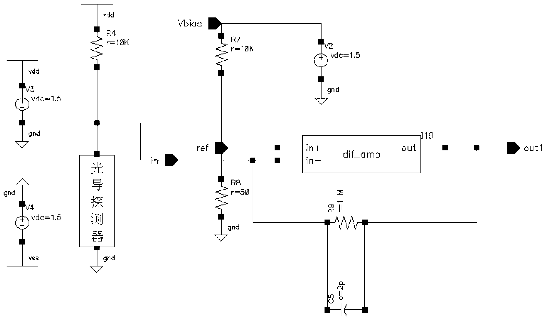
[0015] figure 1 For the bridge mode of the amplifier and the first stage of amplification. R4 is connected with the infrared photoconductive detector. The circuit design is 10K ohms. If you want to increase or decrease the current flowing through the photoconductive detector, you can increase or decrease the resistance of R4. R7 corresponds to R4, and its resistance should be designed to be equal, and this circuit is also designed to be 10K ohms. R8 corresponds to the photoconductive detector, and its size is designed to be equivalent to the resistance of the detector. This circuit is designed to be about 50 ohms. If the resistance of the detector is inconsistent with the size of R8, you can adjust the Vbias to make the output voltage of the circuit be about zero volts when it is static. The amplifier is suitable for amplifying signals of photoconductive detectors with low input impedance of 20 ohms to 200 ohms. When the infrared photoconductive detector receives the infrar...

Embodiment 2

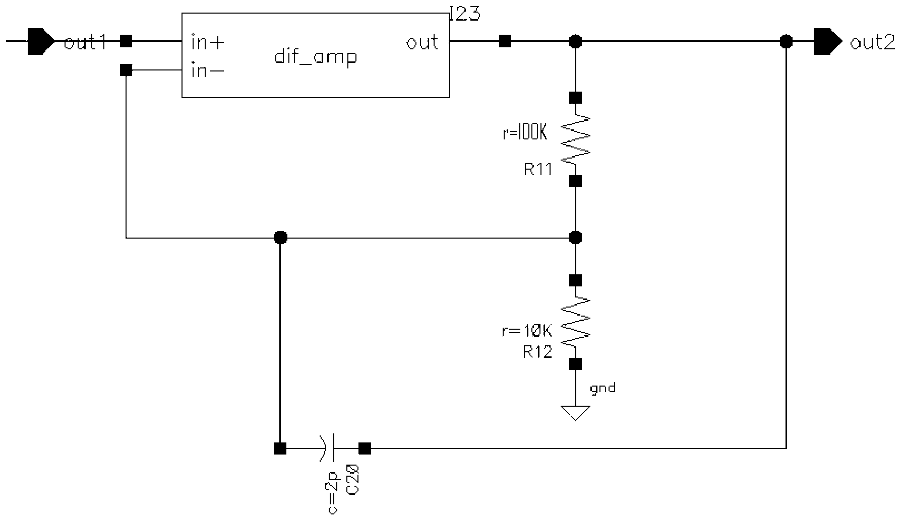
[0019] figure 2 It is a positive terminal amplification method, and its output is in the same phase as the input signal. The ratio of R11 and R12 determines the amplification factor of the second stage. In this circuit, R11 is designed to be 100K ohms, and R12 is designed to be 10K ohms. The magnification is 10x. To increase the magnification of the second stage, the different resistance ratios of R11 and R12 can be changed. The feedback capacitor between the IN negative terminal and OUT is designed to be 2PF. This capacitor acts as a stabilizer for the second circuit. Different magnifications should be compensated with different feedback capacitors.

Embodiment 3

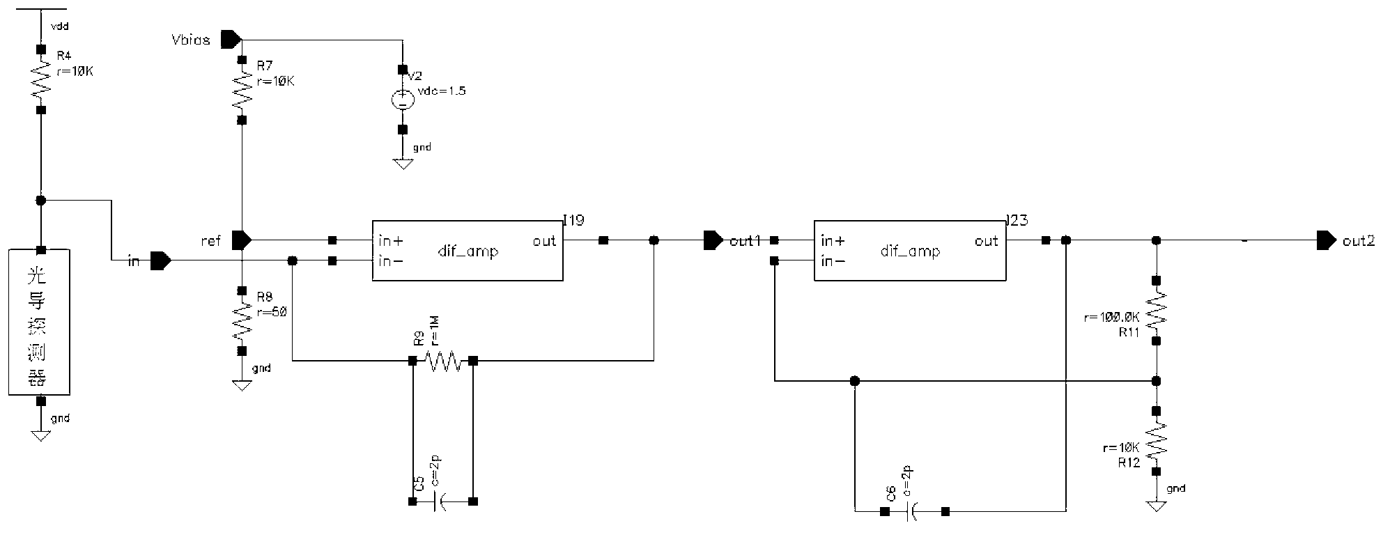
[0021] image 3 It is a general diagram of the connection between the first stage and the second stage. The two-stage amplifiers are directly connected, and the bridge input method and the first-stage amplifier are also directly connected, which overcomes the shortcomings of capacitive coupling. Due to the capacitance The small leakage current will cause the slow drift of the DC static point caused by capacitive coupling. The way of DC connection enables the circuit to amplify both AC and DC signals.


PUM


Abstract

The invention discloses a complementary metal oxide semiconductor (CMOS) amplifying circuit matched with an infrared low-impedance photoconductive detector. The amplifying circuit adopts a bridge circuit mode at an input end, is suitable for amplifying 20-200 ohm low-input-impedance infrared photoconductive detector signals, and can work at liquid nitrogen temperature. A first-level double-end input single-ended output differential amplifier adopts a positive-negative power source for power supply, and enables input quiescent voltage to be free of limitation of the threshold voltage of a metal oxide semiconductor (MOS) transistor. Another branch circuit corresponding to a biasing resistor and the detector adopts 10 kilohms to be connected with 50 ohms in series, the noise rejection ratio led in from another biasing input end is enabled to reach 200 times, and reduction of circuit overall noise is benefited. Under the requirement of a certain bandwidth, in order to increase pre-level gain and lower equivalent input noise, a 1megohm feedback resistor is adopted between a negative input end of the amplifier and output. A direct connection mode is respectively adopted among a bridge input mode, the first-level amplifier and a second-level amplifier, and the amplifiers can amplify both alternate current signals and direct current signals.

Description

technical field [0001] The invention relates to a CMOS circuit design method, in particular to a CMOS amplifying circuit which can work at low temperature and can be matched with a long-wave infrared low-impedance photoconductive detector. Background technique [0002] At present, HgCdTe photoconductive detectors are still the main detectors with wavelengths above 12 microns, and their resistance is very low, about 50 ohms, which is difficult to match with high-resistance CMOS circuits. Some applications even require a wavelength of 15 microns, but no matter how large the detector is, almost all photoconductive detectors are devices without RIOC. Big restrictions. The current infrared focal plane ROIC is almost all for photovoltaic detectors. One of the main reasons why long-wave photoconductive detectors have not achieved focal plane integration is that there is no suitable photoconductive focal plane ROIC. In order to achieve focal plane integration and reduce the overa...

Claims


Application Information

Patent Timeline
IPC IPC(8): H03F3/45
Inventor 袁红辉陈永平陈世军
Owner SHANGHAI INST OF TECHNICAL PHYSICS - CHINESE ACAD OF SCI
Why Eureka
Try Eureka