Preparation method for GaN nanostructure with adjustable Ga vacancy

A nanostructure and vacancy technology, applied in chemical instruments and methods, gaseous chemical plating, crystal growth, etc., can solve the problems of complex preparation process and high cost, and achieve the effect of simple preparation process, less environmental pollution and good uniformity

Inactive Publication Date: 2013-06-26
XINJIANG UNIVERSITY
View PDF3 Cites 4 Cited by
  • Summary
  • Abstract
  • Description
  • Claims
  • Application Information

AI Technical Summary

Problems solved by technology

[0008] The purpose of the present invention is to provide a method for preparing GaN nanostructures with adjustable Ga v

Method used


Image

  • Preparation method for GaN nanostructure with adjustable Ga vacancy
  • Preparation method for GaN nanostructure with adjustable Ga vacancy
  • Preparation method for GaN nanostructure with adjustable Ga vacancy

Examples


Example Embodiment

[0017] Example 1

[0018] Using high-purity Ga 2 o 3 Powder and NH 3 Gas is used as Ga source and N source respectively, according to 0.8 g Ga 2 o 3 The powder is placed in a ceramic boat, and the ceramic boat is placed in the central heating zone, the horizontal tube furnace is sealed, and the vacuum degree is evacuated to 1×10 -2 Below Pa, Ar gas with a flow rate of 100 sccm was introduced to heat the tube furnace. When the temperature reached 980 °C, ammonia gas with a flow rate of 100 sccm was introduced and kept for 3 h. Then, the heating was stopped, the temperature was naturally lowered to 600°C, the heating device was turned on again, and the temperature was raised to 980°C for 2 hours. Finally, turn off the ammonia gas and keep the argon flow constant. Naturally cool to room temperature, turn off the argon, take out the ceramic boat, and obtain sample GaN-1.

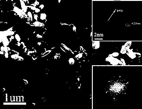
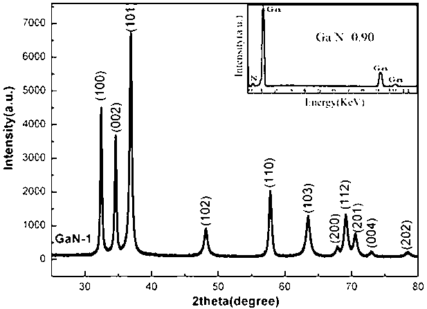
[0019] The XRD spectrum of GaN-1 shows a hexagonal wurtzite structure (ICDD-PDF No. 50-0792), and the...

Example Embodiment

[0020] Example 2

[0021] Using high-purity Ga 2 o 3 Powder and NH 3 Gas is used as Ga source and N source respectively, according to 0.7 g Ga 2 o 3 The powder is placed in a ceramic boat, and the ceramic boat is placed in the central heating zone, the horizontal tube furnace is sealed, and the vacuum degree is evacuated to 1×10 -2 Below Pa, Ar gas with a flow rate of 100 sccm was introduced to heat the tube furnace. When the temperature reached 980 °C, ammonia gas with a flow rate of 150 sccm was introduced and kept for 3 h. Then, the heating was stopped, the temperature was naturally lowered to 600°C, the heating device was turned on again, and the temperature was raised to 980°C for 2 hours. Finally, turn off the ammonia gas and keep the argon flow constant. Naturally cool to room temperature, turn off the argon, take out the ceramic boat, and obtain the sample GaN-2.

Example Embodiment

[0022] Example 3

[0023] Using high-purity Ga 2 o 3 Powder and NH 3 Gas is used as Ga source and N source respectively, according to 0.7 g Ga 2 o 3 The powder is placed in a ceramic boat, and the ceramic boat is placed in the central heating zone, the horizontal tube furnace is sealed, and the vacuum degree is evacuated to 1×10 -2 Below Pa, Ar gas with a flow rate of 100 sccm was introduced to heat the tube furnace. When the temperature reached 980 °C, ammonia gas with a flow rate of 200 sccm was introduced and kept for 3 h. Then, the heating was stopped, the temperature was naturally lowered to 600°C, the heating device was turned on again, and the temperature was raised to 980°C for 2 hours. Finally, turn off the ammonia gas and keep the argon flow constant. Naturally cool to room temperature, turn off the argon, take out the ceramic boat, and obtain the sample GaN-3.

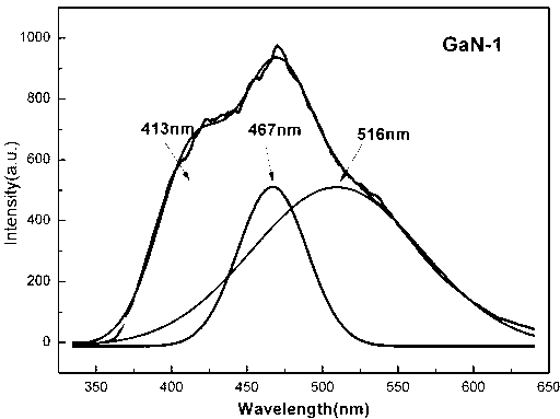
[0024] It can be seen from the above examples that the preparation of GaN nanostructures with adj...


PUM


Abstract

The invention discloses a preparation method for GaN nanostructure with adjustable Ga vacancy, belonging to the field of nanometer materials and a preparation technology thereof. The preparation method adopts a chemical vapor deposition method, and comprises the following steps of taking high purity Ga2O3 powder and NH3 gas as Ga source and N source respectively; putting the Ga2O3 powder in a ceramic boat; putting the ceramic boat at a central heating area; sealing a horizontal tube furnace; vacuumizing till the pressure is below 1*10<-2>Pa, aerating argon of flow of 100sccm, and heating the tube furnace; aerating argon of flow of 100-200sccm at 980 DEG C and keeping aerating for 3 hours; stopping heating, naturally cooling to 600 DEG C, opening a heating device again and heating to 980 DEG C and keeping for 2 hours; and naturally cooling to room temperature, turning off argon and taking a sample out. The preparation method has the characteristics of being simple, low in cost, high in productivity, light in environment contamination, and easy to promote, and the product is uniform and is good in controllability.

Description

technical field [0001] The invention belongs to the technical field of semiconductor nanomaterials and their preparation, relates to dilute magnetic semiconductor materials, and a preparation method of a GaN nanostructure with adjustable Ga vacancies. Background technique [0002] In recent years, dilute magnetic semiconductors (Diluted Magnetic Semiconductors, DMSs), also known as semi-magnetic semiconductors, refer to the doping of a small amount of transition metals or rare earth elements in the matrix of non-magnetic semiconductor materials. Because it can use both the charge characteristics of electrons and the spin characteristics of electrons, it has broad application prospects in the fields of high-density non-volatile memory and semiconductor circuit integrated circuits, semiconductor laser integrated circuits, and quantum computers. [0003] GaN is a direct bandgap semiconductor material with a bandgap width of 3.4eV among III-V semiconductor materials. This type ...

Claims


Application Information

Patent Timeline
IPC IPC(8): C23C16/34C23C16/44C30B29/40C30B25/00
Inventor 吴荣任会会简基康
Owner XINJIANG UNIVERSITY
Why Eureka
Try Eureka