Method for preparing boron-doped diamond and carbon nanotube composite nanocone

A carbon nanotube composite and multi-walled carbon nanotube technology, which is applied in the field of nanomaterials, can solve problems such as non-existence, and achieve the effects of size and density controllability, low field emission threshold voltage, and long emission life

Inactive Publication Date: 2014-12-24
NANJING UNIV OF SCI & TECH
View PDF1 Cites 0 Cited by
  • Summary
  • Abstract
  • Description
  • Claims
  • Application Information

AI Technical Summary

Problems solved by technology

However, there is no preparation technology for boron-doped diamond and carbon nanotube composite nanocones in the prior art

Method used


Image

  • Method for preparing boron-doped diamond and carbon nanotube composite nanocone
  • Method for preparing boron-doped diamond and carbon nanotube composite nanocone
  • Method for preparing boron-doped diamond and carbon nanotube composite nanocone

Examples


preparation example Construction

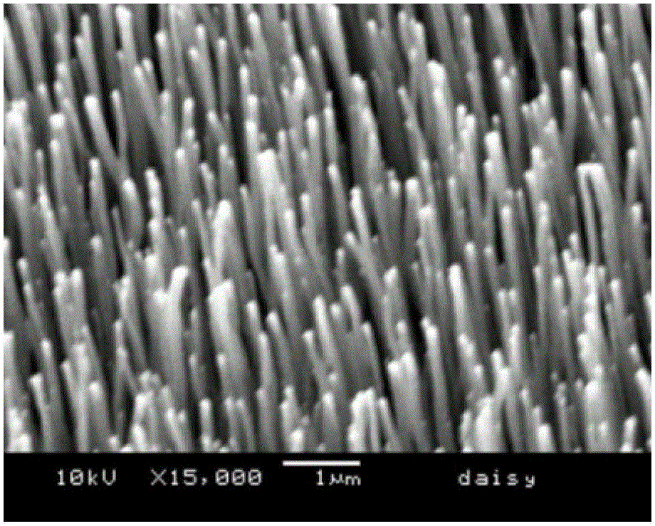
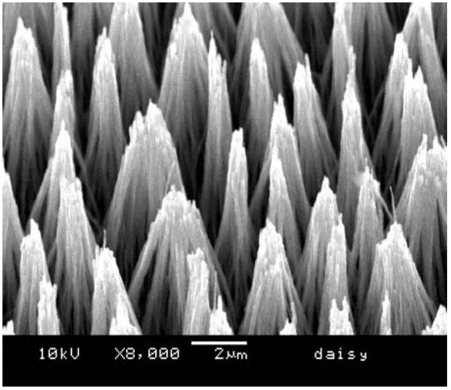
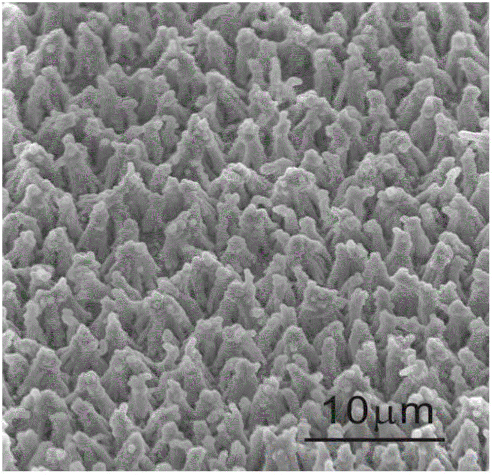
[0019] The invention provides a method for preparing boron-doped diamond and carbon nanotube composite nano-cones. Nano-diamond particles are pre-deposited on the surface of vertically oriented multi-walled carbon nanotubes by electrostatic spraying, and the carbon nano- The tubes are aggregated into a cone-shaped structure; further, a boron-doped diamond film is deposited on the carbon nanotube cone-shaped structure by hot filament chemical vapor deposition to form a composite nanocone of boron-doped diamond and carbon nanotubes with good field emission properties. , including the following steps:

[0020] Step 1, performing surface cleaning treatment on the monocrystalline silicon substrate. The specific operation is: first immerse the substrate in a mixed solution of acetone and ethanol for ultrasonic cleaning, then put it into deionized water for ultrasonic cleaning, and then dry it with cold air;

[0021] Step 2, sequentially sputter deposit a layer of SiO with a thickne...

Embodiment 1

[0028] Multi-walled carbon nanotubes were prepared by plasma-enhanced chemical vapor deposition, and nano-diamond particles were pre-deposited on the surface of vertically oriented multi-walled carbon nanotubes by electrostatic spraying, and the carbon nanotubes were aggregated into cones under the action of electrostatic force Structure; further adopting hot wire chemical vapor deposition method to deposit a layer of boron-doped diamond film on the carbon nanotube cone structure to form a boron-doped diamond and carbon nanotube composite nanocone with good field emission performance, which specifically includes the following steps :

[0029] Step 1, performing surface cleaning treatment on the monocrystalline silicon substrate. The specific operation is: first immerse the substrate in a mixed solution of acetone and ethanol for ultrasonic cleaning, then put it into deionized water for ultrasonic cleaning, and then dry it with cold air;

[0030] Step 2, sequentially sputter d...

Embodiment 2

[0037] Multi-walled carbon nanotubes were prepared by plasma-enhanced chemical vapor deposition, and nano-diamond particles were pre-deposited on the surface of vertically oriented multi-walled carbon nanotubes by electrostatic spraying, and the carbon nanotubes were aggregated into cones under the action of electrostatic force Structure; further adopting hot wire chemical vapor deposition method to deposit a layer of boron-doped diamond film on the carbon nanotube cone structure to form a boron-doped diamond and carbon nanotube composite nanocone with good field emission performance, which specifically includes the following steps :

[0038] Step 1, performing surface cleaning treatment on the monocrystalline silicon substrate. The specific operation is: first immerse the substrate in a mixed solution of acetone and ethanol for ultrasonic cleaning, then put it into deionized water for ultrasonic cleaning, and then dry it with cold air;

[0039] Step 2, sequentially sputter d...


PUM

PropertyMeasurementUnit
thicknessaaaaaaaaaa
thicknessaaaaaaaaaa
diameteraaaaaaaaaa

Abstract

Carbon nanotubes have a relatively high geometric field enhancement effect, low threshold voltage and high field emission performance. Diamond has a negative electron affinity and field emission stability. The two materials can be widely used in field emission display devices. The invention provides a method for preparing a boron-doped diamond and carbon nanotube composite nanocone. By an electrostatic spraying method, a suspension of nanodiamond mixed with methanol is sprayed and coated on vertical orientation growth multi-walled carbon nanotube surfaces to pre-deposite nanocrystalline diamond particles. The adjacent carbon nanotube tips gather into a cone structure under the role of static electricity. Further, a hot filament chemical vapor deposition method is used for depositing a layer of boron-doped diamond thin film on carbon nanotube cone structures to form the neat, uniform, and size and density-controllable boron-doped diamond and carbon nanotube composite nanocone. The composite nanocone has the advantages of low field emission threshold voltage, long electron emission life and stable performance, and can be applied to field emission devices, electrochemical electrodes and hydrogen storage devices.

Description

technical field [0001] The invention relates to nanometer material technology, in particular to a method for preparing a boron-doped diamond and carbon nanotube composite nanocone that can be applied to high-performance and long-life field emission devices, electrochemical electrodes and hydrogen storage devices. Background technique [0002] Carbon nanotubes have a small radius of curvature at the tip, a large aspect ratio, excellent mechanical properties, good chemical stability and electrical conductivity, so they have a high end geometric field enhancement effect, low threshold voltage and efficient field emission performance. Since their discovery, there has been great interest in the application of carbon nanotubes as electron sources to field emission display devices. The field emission research of single and multiple carbon nanotubes and carbon nanotube films has received widespread attention. However, the field emission current of carbon nanotubes is unstable and th...

Claims


Application Information

Patent Timeline
Patent Type & Authority Patents(China)
IPC IPC(8): C01B31/02C23C16/44C23C16/26C23C16/27B82Y40/00B82Y30/00C01B32/15C01B32/158C01B32/25
Inventor 邹友生顾磊张亦弛何林林朱正峰石晓琴
Owner NANJING UNIV OF SCI & TECH
Why Eureka
Try Eureka