Super wide band cut-off long-wave-pass filter optical film and production method thereof
A manufacturing method and technology of filter film, applied in the direction of optical filter, optics, optical components, etc., can solve the problems of high passband transmittance, long plating cycle, not steep transition zone, etc., to improve adhesion and the quality of film-forming products, eliminate the cumulative error of film thickness, and ensure the effect of optical performance
- Summary
- Abstract
- Description
- Claims
- Application Information
AI Technical Summary
Problems solved by technology
Method used
Image
Examples
Embodiment 1
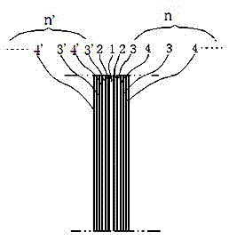
[0036] Example 1 :Such as figure 1 Shown is a basic embodiment of an ultra-broadband cut-off long-pass filter film of the present invention. An ultra-broadband cut-off longwave pass filter film, which includes a substrate 1, the substrate 1 is an optical element, its front and back sides are respectively coated with transition bonding layers 2, and the transition bonding layers 2 are alternately coated There are several layers of long-wave pass filter films with different central wavelengths, forming two long-wave pass filter films: one is the long-wave pass filter film n on the front of the substrate, and the other is the long-wave pass filter n' on the back of the substrate. , the two long-wave pass filter film systems are composed of a high refractive index layer and a low refractive index layer, figure 1 Middle: The long-wave pass filter film system n on the front of the substrate is composed of a high-refractive index layer 3 and a low-refractive-index layer 4, and the...
Embodiment 2
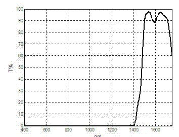
[0037] Example 2 : Different from the above-mentioned embodiment 1: the material of the substrate 1 is mainly selected from colored glass or infrared crystal; the material of the transition bonding layer is SiO 2 , or SiO, or Al 2 o 3 , the high refractive index material is TiO 2 , or Ta 2 o 5 , the low refractive index material is SiO 2 . The cut-off bands of the two long-wave pass filter films n and n' are completely connected in series, and there is a cut-off overlapping area of 10-50nm; wherein, the short-wave cut-off point of the long-wave pass filter film with a smaller central wavelength is smaller than the optical cut-off point. The upper limit of the intrinsic absorption cutoff of the component. The optical element after the long-wave pass filter film is finally formed has the optical characteristics of cut-off from the depth of the 400-1400nm band and the transmittance of the 1500-1700nm band not less than 92%.
Embodiment 3
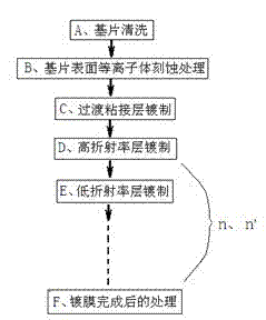
[0038] Example 3 :Such as figure 2 Shown is a basic embodiment of the method for manufacturing an ultra-broadband cut-off long-pass filter film of the present invention. The manufacturing method of the ultra-broadband cut-off long-wave pass filter film of the present invention, its manufacturing steps include: A, substrate cleaning, B, substrate surface plasma etching treatment, C, transition bonding layer plating, D , high-refractive-index layer plating, E, low-refractive-index layer plating, F, the treatment after the coating is completed; The film thickness real-time monitoring method is to plate long-wave pass filter films with different center wavelengths on the front and back of the substrate respectively to form two long-wave pass filter film systems, one is the long-wave pass filter film system n on the front of the substrate, and the other is The long-wave pass filter film system n' on the reverse side of the substrate; the monitoring chip replacement strategy ref...
PUM
 Abstract
Description
Claims
Application Information


