Double-junction depth photodiode for fluorescence detection

A photodiode and deep junction technology, applied in the field of fluorescence detection photosensitive sensing units, can solve the problems of narrow spectral response range, wide spectral response range, and large dark current noise, and achieve high sensitivity, wide spectral response, and low dark current. Effect

Active Publication Date: 2013-07-24
ZHEJIANG UNIV OF TECH
View PDF4 Cites 10 Cited by
  • Summary
  • Abstract
  • Description
  • Claims
  • Application Information

AI Technical Summary

Problems solved by technology

[0005] In order to solve the shortcomings of low quantum efficiency, large dark current noise, and narrow spectral response range of single-junction deep PN junction photoelectric conversion in fluorescence detection, the invention provides a double-junction deep PN junction photodiode based on standard CMOS technology, With higher photoelectric conversion sensitivity, smaller dark current noise and wider spectral response range

Method used


Image

  • Double-junction depth photodiode for fluorescence detection
  • Double-junction depth photodiode for fluorescence detection
  • Double-junction depth photodiode for fluorescence detection

Examples


Embodiment

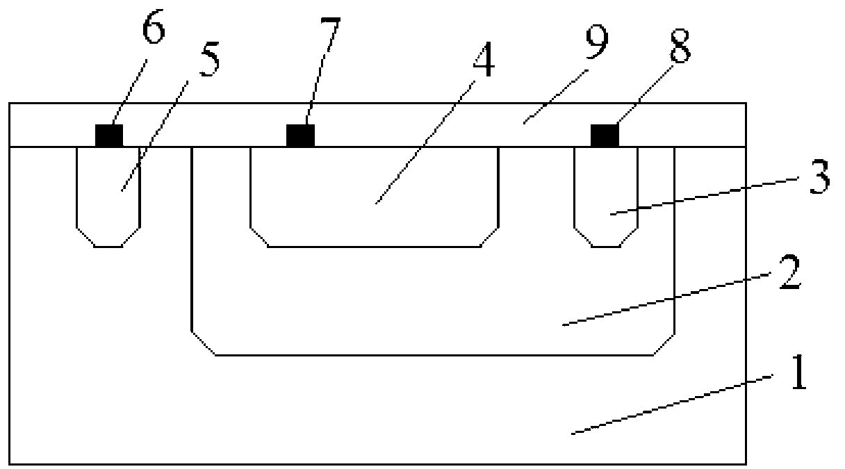
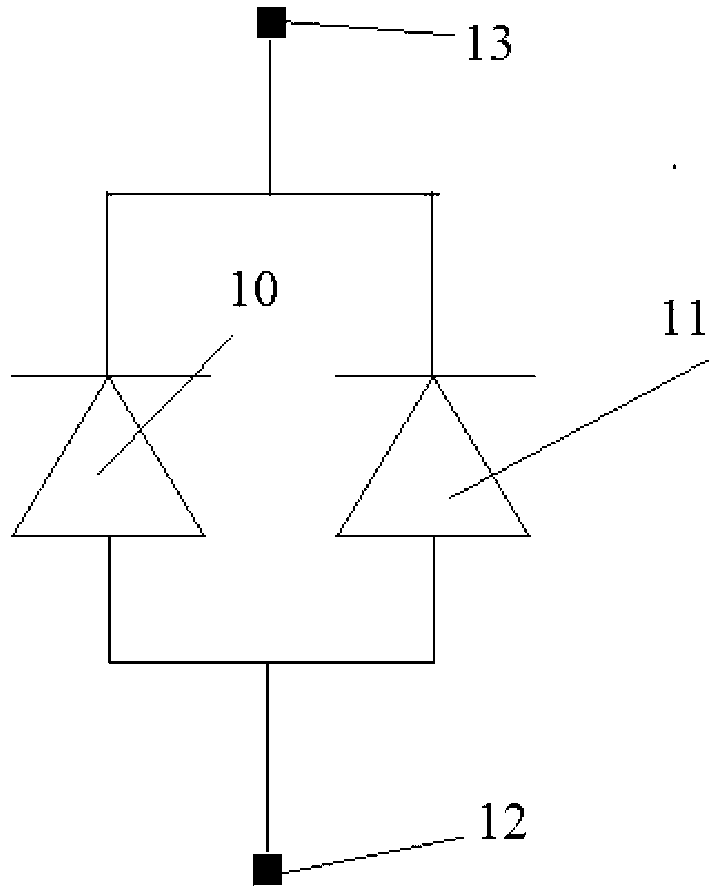
[0017] refer to figure 1 , a double-junction deep PN junction photodiode based on a standard CMOS process, comprising a deep junction PN junction photodiode composed of a semiconductor silicon P-type substrate 1 and an N-type well 2; a P-type source-drain injection 4 and the N-type well Shallow junction PN junction photodiode composed of type well 2. The semiconductor silicon P-type substrate 1 is the anode of the deep-junction PN junction photodiode, and the N-type well 2 is the cathode of the deep-junction PN junction photodiode; the P-type source-drain injection 4 is the The anode of the shallow junction PN junction photodiode, the N-type well 2 is the cathode of the shallow junction PN junction photodiode. The semiconductor silicon P-type substrate 1 forms a heavily doped ohmic contact through a P-type source-drain implant 5, and leads out through a metal contact hole 6, and the N-type well 2 forms a heavily-doped ohmic contact through an N-type source-drain implant 3 , ...


PUM


Abstract

The invention relates to a double-junction depth PN junction photodiode based on standard CMOS (Complementary Metal Oxide Semiconductor) technology. The double-junction depth PN junction photodiode comprises a deep junction PN junction photodiode and a shallow junction PN junction photodiode, wherein the deep junction PN junction photodiode is composed of a semiconductor silicon P type substrate and an N type well, and the shallow junction PN junction photodiode is composed of a P type source-drain injection region and the N type well; the semiconductor silicon P type substrate is an anode of the deep junction PN junction photodiode, and the N type well is a cathode of the deep junction PN junction photodiode; the P type source-drain injection region is an anode of the shallow junction PN junction photodiode, and the N type well is a cathode of the shallow junction PN junction photodiode; the semiconductor silicon P type substrate form heavily doped ohmic contact through the P type source-drain injection region, and is leaded out through a metallic contact hole; and the N type well forms heavily doped ohmic contact through an N type source-drain injection region, and is leaded out through a metallic contact hole.

Description

technical field [0001] The invention relates to a double-junction deep photodiode, which has higher sensitivity and wider spectral response than a single-junction deep photodiode, is compatible with standard CMOS technology, and can be used as a fluorescence detection in biomedicine, food safety and environmental monitoring Photosensitive sensing unit. Background technique [0002] In 1852, British physicist and mathematician G.G. Stokes (G.G.Strokes) discovered fluorescence, and proposed that fluorescence is a kind of photoluminescence phenomenon, which is the light radiation emitted by substances after absorbing photons. For a dilute solution of a fluorescent substance, under the irradiation of excitation light, the fluorescence intensity of the measured solution is proportional to the concentration of the fluorescent substance. By measuring the fluorescence intensity, many substances related to life science can be quantified, such as amino acids, amines, Vitamins and met...

Claims


Application Information

Patent Timeline
Patent Type & Authority Applications(China)
IPC IPC(8): H01L27/142
CPCY02E10/50
Inventor 施朝霞
Owner ZHEJIANG UNIV OF TECH
Why Eureka
Try Eureka