Measuring device and measuring method for tiny surface defect through post-magnification digital holographic microscopy

A digital holographic microscope and measuring device technology, which is applied in the direction of measuring devices, optical devices, and optical testing of flaws/defects. It can solve problems such as low precision, high labor costs, and slow detection speed, and achieve good dynamic performance. Effect of suppressing stray light and improving signal-to-noise ratio

Inactive Publication Date: 2013-07-31
SHANGHAI UNIV
View PDF4 Cites 9 Cited by
  • Summary
  • Abstract
  • Description
  • Claims
  • Application Information

AI Technical Summary

Problems solved by technology

However, the shortcomings of this method are also obvious: human subjectivity factors, the size of the defect cannot be quantified, the detection speed is slow, the labor cost is high, and the observer needs to be trained; 2) The filter imaging method is different from the visual method. The principle is exactly the same, the only difference is that the human eye is replaced by an optical sensor array, which eliminates the subjectivity of human eye judgment, improves the detection speed, and can quantify the detection results
Its disadvantage is that the detection accuracy is not high, and it is easily affected by the environment such as light; 3) Diffuse scattered light receiving method
Its advantage is that the location of the defect is accurate; the disadvantage is that it cannot accurately reflect the size of the defect; 4) Diffraction light intensity method
Its advantage is that the error is small; the disadvantage is that it is only for the defect of a specific shape; 5) laser spectrum method
Its advantage is that it has high sensitivity; but it only detects defects of specific shapes

Method used


Image

  • Measuring device and measuring method for tiny surface defect through post-magnification digital holographic microscopy
  • Measuring device and measuring method for tiny surface defect through post-magnification digital holographic microscopy
  • Measuring device and measuring method for tiny surface defect through post-magnification digital holographic microscopy

Examples


Embodiment 1

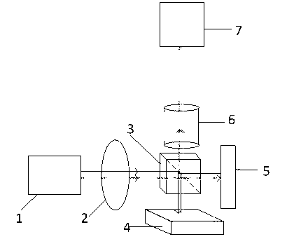
[0021] Such as figure 1 As shown, a post-magnification digital holographic microscopic surface micro-defect measurement device includes a laser 1, a convex lens 2, a first dichroic prism 3, a reference mirror 5, a microscopic objective lens 6 and a CCD camera 7; the convex lens 2, the first The horizontal central axis of a dichroic prism 3 and the reference mirror 5 is on the same horizontal straight line as the central axis of the light beam emitted by the laser 1; The camera 7 is on the same vertical line, and the central axis of the light beam sent by the laser intersects the central point of the beam splitting prism; the vertical central axis of the laser 1, the convex lens 2 and the first beam splitting prism 3 are parallel to each other; the first beam splitting The horizontal central axes of the prism 3, the microscopic objective lens 6 and the CCD camera 7 are parallel to each other.

[0022] Such as image 3 As shown, a post-amplification digital holographic microsc...

Embodiment 2

[0025] This embodiment is basically the same as Embodiment 1, the difference is:

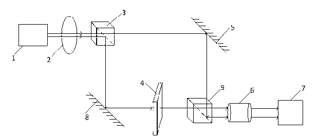
[0026] Such as figure 2 As shown, the device also includes a reflecting mirror 8 and a second dichroic prism 9; the horizontal central axis of the convex lens 2 and the first dichroic prism 3 is on the same horizontal straight line as the central axis of the beam emitted by the laser 1; 8. The position to be detected of the workpiece 4 to be measured, the horizontal central axis of the second dichroic prism 9, the microscopic objective lens 6 and the CCD camera 7 are on the same horizontal straight line as the central axis of the measuring beam; the mirror 8 is 45 to the horizontal axis Placement; the vertical central axes of the laser 1, the convex lens 2, the first beam splitting prism 3, the workpiece to be measured 4, the second beam splitting prism 9, the microscopic objective lens 6 and the CCD camera 7 are parallel to each other.

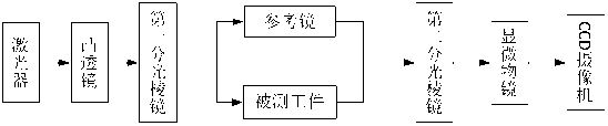
[0027] Such as Figure 4As shown, the method also incl...


PUM


Abstract

The invention relates to a measuring device and a measuring method for a tiny surface defect through post-magnification digital holographic microscopy. The measuring method comprises the steps that a short coherent light source is adopted; scattered light information of the tiny surface defect of an optical element is obtained in an oblique incidence manner; scattered light interferes with a reference beam; interference image information is magnified in a post-magnification manner and received by a CCD (Charge Coupled Device) camera; and finally a pattern of the tiny surface defect and quantification information of depth distribution are computed and analyzed through a digital holographic principle. The device is mainly used for achieving detection of the tiny surface defect of the smooth optical element. The device can obtain depth and phase information of the surface defect by acquiring a single image and conducting related processing, can distinguish surface dust and indentation of the optical element, and can dynamically and rapidly measure. The device adopts a parallel light irradiation and off-axis holographic technique, and forms a post-magnification digital holographic recording system, so that the device is good in dynamic property and has the characteristics of non-destruction and information quantification.

Description

technical field [0001] The invention relates to a post-magnification digital holographic microscopic surface micro-defect measurement device and method. Background technique [0002] The processing quality evaluation of the surface of precision optical components mainly includes four main aspects: surface shape detection, surface roughness detection, surface waviness detection and surface defect detection. Surface shape deviation refers to the difference between the surface shape to be processed and the actual surface shape. Its horizontal scale is on the order of millimeters, which belongs to the macro-scale deviation. Usually, the interference fringes formed by the superposition of the measured wave surface and the standard wave surface are used for inversion. , so as to obtain this deviation. Surface roughness refers to the microstructure of the processed surface with small spacing and peak-to-valley values. For the surface of precision optical components, the lateral sc...

Claims


Application Information

Patent Timeline
Patent Type & Authority Applications(China)
IPC IPC(8): G01B9/021G01N21/88
Inventor 于瀛洁涂桥伍小燕周文静
Owner SHANGHAI UNIV
Why Eureka
Try Eureka