

Active driving wire cable table of silicon wafer stage of lithography machine
A technology of active drive and silicon wafer stage, which is applied in the direction of microlithography exposure equipment, photolithography exposure device, etc., can solve the problems of complex cable stage structure, high development cost, and large number of drivers, and achieve mechanical structure and control. The algorithm is simple, the motion positioning accuracy is improved, and the scalability is good.
- Summary
- Abstract
- Description
- Claims
- Application Information
AI Technical Summary
Problems solved by technology
Method used
Image

Examples
Embodiment Construction
[0030] In order to better understand the technical content of the present invention, specific embodiments are given together with the attached drawings for description as follows.
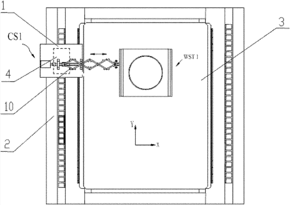
[0031] The present invention proposes a silicon wafer table cable table that adopts a cross-telescopic linkage mechanism for photolithography machines, and is especially suitable for a workpiece table motion system that uses a planar motor to realize long-stroke rough motion of a silicon wafer table. The H-frame dual workpiece system is also suitable.
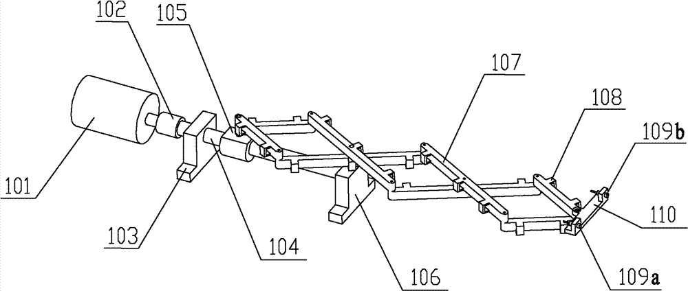
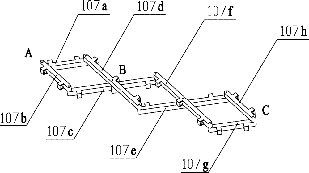
[0032] figure 1 Shown is a schematic structural diagram of the actively driven cable stage of the silicon wafer stage of the photolithography machine according to Embodiment 1 of the present invention. figure 2 Shown is the schematic diagram of the cross-telescopic linkage mechanism installed on the lead screw nut in embodiment 1; image 3 Shown is a schematic diagram of the cross-telescopic linkage mechanism in Embodiment 1. Please also refer t...
PUM
 Abstract
Description
Claims
Application Information