[0035] The present invention will be further described below in conjunction with the drawings and specific implementations.
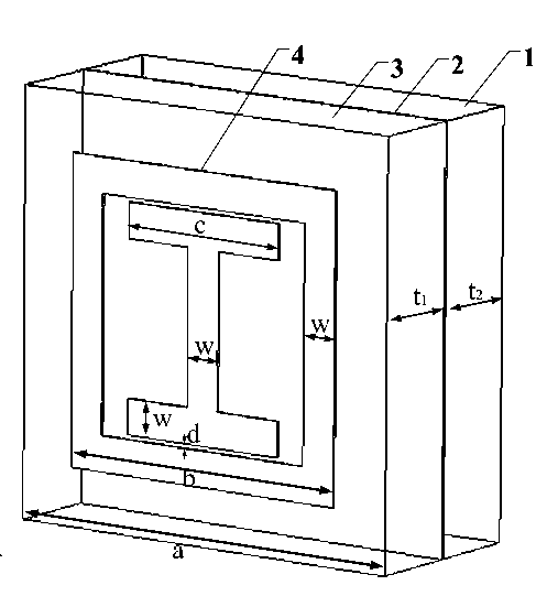
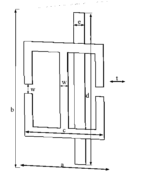
[0036] The bottom layer provided by the present invention is a continuous metal film, the middle is a dielectric layer, and the surface layer is a metamaterial structure composed of two parts of metal "I" on the inside and a "box" on the periphery, which has a special terahertz response performance. The embodiment of the present invention for making the metamaterial structure is as follows: (1) A single crystal silicon wafer is selected as the substrate 1 of the metamaterial, and after cleaning, it is dried with high-purity nitrogen for use; (2) On the surface of the substrate 1, A continuous gold film with a thickness of 5~2000 nm is deposited using an electron beam evaporation system as the underlying metal 2 of the metamaterial; (3) On the surface of the continuous gold film 2 described above, a layer with a thickness of 0.05~40 μm is spin-coated Polyimide film, as the dielectric layer 3 of the metamaterial; (4) On the surface of the polyimide film 3, the second layer of gold film 4 of the metamaterial is deposited by the electron beam evaporation system, with a thickness of 5~2000 nm; (5) Using the etching method, through the mask, according to the set size (a=36μm, b=26μm, c=14.8μm, d=0.4μm, t 1 =8μm, t 2 =8μm, the cell area is 26mm×26mm), the second layer of metal 4 is selectively etched until the polyimide layer 3 underneath is exposed, forming a gold with "I" inside and "frame" outside The pattern constitutes the surface resonator of the metamaterial, thereby preparing the metamaterial. When the thickness of the metamaterial thus prepared is 200nm (Au)/8000nm (polyimide)/200nm (Au), the central absorption frequency at the low frequency end is 1.81 THz, and the response frequency band with an absorption rate greater than 90% is 57.4 GHz.
[0037] figure 1 It is a unit structure of terahertz metamaterials that meets the impedance matching conditions proposed by the present invention. Its bottom layer is a continuous metal film, and the surface metal film is patterned into a two-piece structure with a “I-shape” on the inside and a “box” on the periphery. Part of the resonator, the middle of the two layers of metal is a dielectric layer. The original cell size of the metamaterial is a=36μm, b=26μm, c=14.8μm, d=0.4μm, t 1 =8μm, t 2 =8μm, the original unit area is 26mm×26mm.
[0038] As a comparison, figure 2 Show a traditional metamaterial structure with a metal resonator on the surface, a dielectric layer in the middle, and a linear metal bottom layer. figure 2 The original unit of the structure has a width a=34mm and a length b=50mm. From top to bottom, the surface layer is an electrical resonator structure layer. The length and width of the electrical resonator are c=30mm, and the line width and opening are w=3mm; the middle layer is a polyimide dielectric layer with a thickness of t=8mm ; The bottom layer is a metal wire, the metal wire is trapped in polyimide, its length d=48mm, width e=4mm; the surface electric resonator and the bottom metal wire are both Au, and the thickness is 200nm.
[0039] For what the present invention mentions figure 1 In the metamaterial structure shown, the dielectric layer in the middle is not particularly limited. In addition to the polyimide film, it can also be silicon nitride (SiN) of different thickness and composition. x ) Thin film, amorphous silicon (a-Si) film, silicon oxide (SiO x ) Film, silicon oxynitride (SiN x O y ) Film, or aluminum oxide (AlO x ) Film, hafnium oxide (HfO x ) Membrane, hafnium alumina (HfAlO x ) One of the membranes, or their composite membranes. Proposed by the present invention figure 1 The metal of the surface layer and the bottom layer of the metamaterial structure shown is also not particularly limited, and can be metal Au, or metal Al, Ti, TiN x , TiSi x , TiW x , W, WSi x , Ni, NiSi x , Ta, TaN x , Fe, Pt, Cu, Ag, NiCr x One of the alloys, or a mixture of several metals. Proposed by the present invention figure 1 The substrate of the metamaterial shown is also not particularly limited. It can be a single crystal silicon wafer, or a silicon nitride film, an amorphous silicon film, a silicon oxide film, a silicon oxynitride film, a polyimide film, or polyethylene. One of film, polystyrene film, polypropylene film, gallium arsenide film, and composite film of these materials. The metamaterial structure that satisfies the regulation law proposed by the present invention is also not particularly limited, and may be figure 1 The metamaterial structure proposed by the present invention shown, figure 2 The traditional metamaterial structure shown is one of the other metamaterial structures known in the industry.
[0040] The analysis of the following methods can prove that the method of adjusting the entire metamaterial unit structure according to the present invention can effectively adjust the terahertz center absorption frequency, response frequency band, and film thickness of the metamaterial. The need for uncooled terahertz detectors.
[0041] Use the frequency domain algorithm in CST Microwave Studio2011 electromagnetic simulation software to analyze the metamaterial structure proposed in the present invention ( figure 1 ) For calculation, the structural unit X and Y direction boundaries are set as (unit cell) periodic boundaries, that is, the structural units are arranged infinitely in the X and Y directions, and the wave vector K is along the Z direction. Assuming that the transmission is zero, the absorptivity can be passed A(ω)=1-|S 11 |2 -|S 12 | 2 get. The simulation parameters include: the dielectric constant of polyimide is 3.5, the loss tangent is 0.0027, and the conductivity of the Au film is δ=4.561×10 7. image 3 For the present invention figure 1 As shown in the metamaterial, when the bottom and surface layers are made of Au film, and the dielectric layer is made of polyimide film, the original film thickness is 200nm (Au)/8000nm (polyimide)/200nm (Au), and the figure 1 The simulation results of the terahertz absorption rate of the metamaterial at different frequencies with the original cell size and the original cell area shown. image 3 It is shown that in the frequency range of 1-3 THz, the metamaterial structure proposed by the present invention ( figure 1 ) Has two absorption peaks. Among them, the center absorption frequency of the low frequency end is 1.81 THz, its absorption rate is nearly 100%, and the response frequency band (defined as the frequency range with an absorption rate greater than 90%) is 57.4 GHz.
[0042] For what the present invention mentions figure 1 For the metamaterial structure, while other parameters remain unchanged, if only one structural parameter of the thickness of the dielectric layer is changed, for example, the thickness of the dielectric layer is changed from the original 8 mm ( figure 1 ) Is reduced to 6 mm, the parameter change will cause the structure to change the response effect of the terahertz, the terahertz absorption of the structure after the thickness of the dielectric layer is changed is shown in Figure 4a. Figure 4-a It is shown that after the medium thickness becomes thinner (6 mm), the central absorption frequency of the structure becomes 1.79 Hz (previously 1.81 THz); in addition, due to the enhancement of reflection, the absorption peak is reduced from 98.4% before the change to 90.4%. In the other case, when other parameters remain unchanged, if only the figure 1 The outer frame size of the metamaterial electric resonator is changed from 26mm×26mm to 28mm×28mm, while the shape, position and other structural parameters of the I-type resonator remain unchanged. After this size change, the terahertz absorption of the metamaterial is shown in Figure 4b. Figure 4-b It shows that the absorption frequency of the structure (28mm×28mm) at this time is 1.79 THz (the original 26mm×26mm is 1.81 THz), and the absorption rate is significantly reduced from nearly 100% before the change to 72.3% (Figure 4b). Figure 4-a and 4-b The results show that if only one structural parameter of the metamaterial is changed, the impedance matching of the original structure will be destroyed and the terahertz absorption rate of the metamaterial will be significantly reduced. If it is necessary to regain the high absorption rate, other structural parameters need to be coordinated and optimized systematically, so as to re-establish impedance matching and obtain high terahertz absorption rate. It can be seen that the traditional method of adjusting and controlling the structural parameters of metamaterials is cumbersome, time-consuming, and uncertain.
[0043] Figure 5 is the use of the regulation method proposed by the present invention, figure 1 The terahertz response of the unit structure of the metamaterial shown as a whole is reduced or enlarged. E.g, Figure 5-c It shows that when the structural unit is reduced to 1/2 of the original size (ie a=18μm, b=13μm, c=7.4μm, d=0.2μm, t 1 =4μm, t 2 =4μm, the thickness of the gold film becomes 100nm, the thickness of the polyimide dielectric layer becomes 4000nm, and the cell area is 13mm×13mm), the central absorption frequency of the new structure becomes 3.59 THz, which is the original response frequency (1.81 THz) 2 times. Moreover, the absorption peak at 3.59 THz is close to 100%, and the response band with an absorption rate greater than 90% is 148 GHz, which is also significantly wider than the 57.4 GHz before adjustment. Other changes in the overall ratio of the metamaterial unit structure, such as (a) 2 times, (b) 3/2 times, (d) 1/5 times, see the simulation results Figure 5-a , 5-b , 5-d. After the unit structure is reduced or enlarged as a whole, the terahertz absorption rate of the metamaterial is between 99.09% and 99.98%, which is almost "perfect absorption", indicating that if the method shown in the present invention is used to scale the structural unit as a whole, The impedance matching of the structure will not be destroyed, so the high terahertz absorption characteristics of the metamaterial are maintained. And it clearly shows that after the overall structure is reduced, the terahertz center absorption frequency of the metamaterial will move to the high frequency direction, and the response frequency band will become wider. The changes in the absorption frequency and response frequency band of the metamaterials caused by this regulation conform to certain laws.
[0044] In order to further reveal the law of changes in metamaterial properties caused by the regulation method proposed in this patent, we combine the figure 1 The unit structure of the metamaterial shown is scaled from 0.2 times to 2 times as a whole, and then the scaled terahertz response is simulated and calculated systematically. The changes in the central absorption frequency of the metamaterial caused by the overall scaling of the unit structure are summarized in Image 6 in. Image 6 It is shown that when the zoom ratio changes from 0.2 times to 2 times, the central absorption frequency of the metamaterial gradually decreases from 8.910 THz to 0.906 THz. according to Image 6 As a result, we concluded that the terahertz response frequency of the metamaterial caused by the overall scaling method of the unit structure proposed in this patent satisfies f 2 =f 1 /k law, where k is the overall reduction or enlargement of the metamaterial unit, f 1 Is the central absorption frequency of the structure before the change, f 2 Is the central absorption frequency of the structure after the change. Figure 7 According to the regulation method proposed by the present invention, figure 1 The metamaterial unit structure is scaled as a whole, and the absorption peak of the structure with a scaling ratio of 0.2 to 2 and the change of the response frequency band with an absorption rate greater than 90%. Figure 7 It shows that when the zoom ratio is changed from 0.2 times to 2 times, the peak response frequency of the metamaterial varies between 98.59% and 99.99%, almost all of which are "perfect absorption"; moreover, the terahertz response frequency band of the metamaterial varies with the unit structure The overall enlargement and narrowing, and the overall reduction and widening of the unit structure.
[0045] According to the method for adjusting and controlling the overall scaling of the unit structure provided by the present invention, figure 2 The traditional metamaterial structure with metal wires as the bottom layer is also controlled in the same way. When the overall zoom ratio of this traditional metamaterial unit structure changes from 0.2 times to 2 times, the response frequency of the metamaterial changes from 5.540 THz is gradually reduced to 0.569 THz, and the absorption rate varies between 90.8% and 99.1%, which is similar to that of the metamaterial shown in the present invention. Image 6 result. The change law of absorption peak and response frequency band of the traditional metamaterial structure is similar to that of the metamaterial shown in the present invention. Figure 7 result. The simulation results of other metamaterial structures also show similar changes. These results indicate that the control method provided by the present invention has a general rule in the terahertz response of metamaterials.