Silicon single crystal manufacturing method, silicon single crystal and wafer

A silicon single crystal and wafer technology, which is applied in the direction of single crystal growth, single crystal growth, chemical instruments and methods, etc., can solve the problems of inability to achieve radial uniformity of resistivity and change of wafer resistivity.

Active Publication Date: 2016-08-17
SILTRONIC AG
View PDF11 Cites 0 Cited by
  • Summary
  • Abstract
  • Description
  • Claims
  • Application Information

AI Technical Summary

Problems solved by technology

[0006] However, the above-mentioned conventional techniques cannot achieve the tighter radial uniformity of resistivity and the variation of resistivity between wafers, which are required for silicon single crystal wafers for power device applications

Method used


Image

  • Silicon single crystal manufacturing method, silicon single crystal and wafer
  • Silicon single crystal manufacturing method, silicon single crystal and wafer
  • Silicon single crystal manufacturing method, silicon single crystal and wafer

Examples


Embodiment

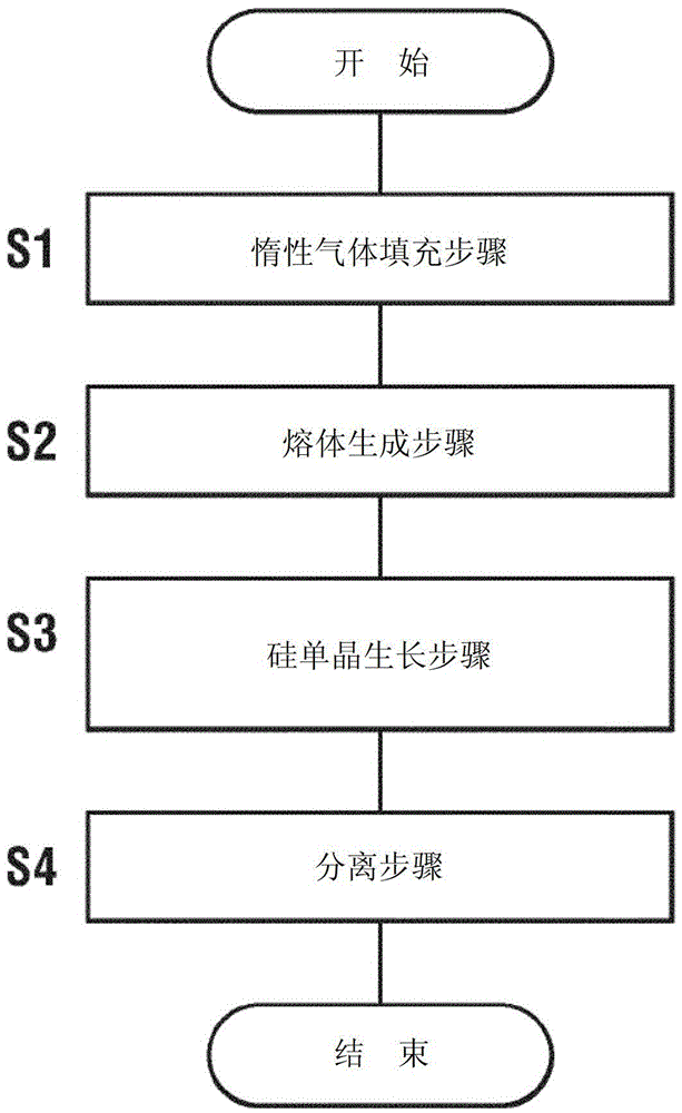
[0081] Examples and comparative examples of the silicon single crystal production method according to this embodiment of the present invention are described below.

[0082] Manufacture of silicon single crystal

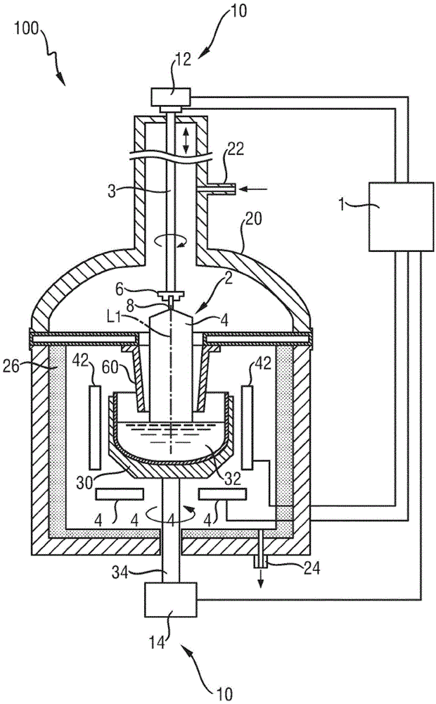
[0083] An apparatus for producing a silicon single crystal by the CZ method was used to grow a silicon single crystal (ingot) with a diameter of 200 mm.

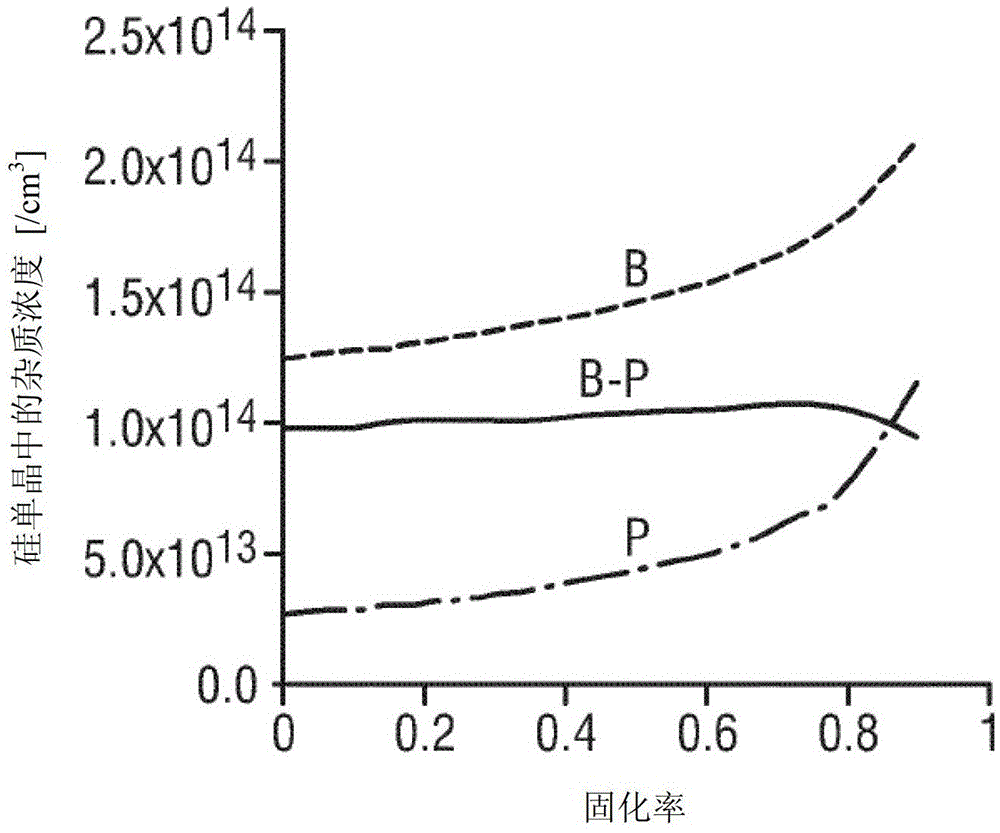
[0084] Here, an initial silicon melt has a boron concentration and a phosphorus concentration as shown below, and a seed crystal is immersed in the initial silicon melt to grow a silicon single crystal. The crystal growth rate was set at 0.9 mm / min, and the cooling rate at the edge portion of the crystal was set at 1.9 times the cooling rate at the central portion of the crystal.

[0085] (1) Embodiment 1

[0086] Addition of boron and phosphorus to the nascent silicon melt, resulting in a boron concentration of 1.6E14 atoms / cm 3 , the phosphorus concentration reaches 7.2E13 atoms / cm 3 (The ratio of phosphorus c...

Embodiment 2

[0088] Boron and phosphorous are added to the nascent silicon melt, resulting in a boron concentration of 4.0E14 atoms / cm 3 , the phosphorus concentration reaches 1.8E14 atoms / cm 3 (The ratio of phosphorus concentration to boron concentration is 0.45).

Embodiment 3

[0090] Boron and phosphorus are added to the nascent silicon melt to bring the boron concentration to 1.1E14 atoms / cm 3 , the phosphorus concentration reaches 4.6E13 atoms / cm 3 (The ratio of phosphorus concentration to boron concentration is 0.42).

[0091] (4) Embodiment 4

[0092] Addition of boron and phosphorus to the nascent silicon melt, resulting in a boron concentration of 1.6E14 atoms / cm 3 , the phosphorus concentration reaches 7.5E13 atoms / cm 3 (The ratio of phosphorus concentration to boron concentration is 0.47).

[0093] (5) Example 5

[0094] Addition of boron and phosphorus to the nascent silicon melt, resulting in a boron concentration of 1.6E14 atoms / cm 3 , the phosphorus concentration reaches 8.0E13 atoms / cm 3 (The ratio of phosphorus concentration to boron concentration is 0.50).

[0095] (6) Comparative Example 1

[0096] Boron is added to the nascent silicon melt to achieve a boron concentration of 1.0E14 atoms / cm 3 .


PUM

PropertyMeasurementUnit
electrical resistivityaaaaaaaaaa

Abstract

Provided is a silicon single crystal manufacturing method for manufacturing a p-type silicon single crystal by the Czochralski method, from which a wafer with high resistivity, good radial uniformity of resistivity and little variation in resistivity can be obtained. The p-type silicon single crystal 2 is grown by the Czochralski method from an initial silicon melt in which the boron concentration is not more than 4E14 atoms / cm3 and the ratio of phosphorus concentration to boron concentration is not less than 0.42 and not more than 0.50.

Description

technical field [0001] The present invention relates to a silicon single crystal manufacturing method, a silicon single crystal and a wafer, in particular to a method for manufacturing a silicon single crystal, a silicon single crystal and a wafer by the Czochralski method. Background technique [0002] Power devices installed in automobiles, home appliances, etc. should have high withstand voltage, and the resistance of the substrate affects their characteristics. Therefore, a silicon wafer used as a substrate is required to have high resistivity with little variation. [0003] If a p-type silicon single crystal is grown by the Czochralski method in which boron is added as an impurity, since the segregation coefficient of boron to the silicon single crystal is less than 1, boron is concentrated in the silicon melt during single crystal growth. The boron concentration in the silicon single crystal then increases as the single crystal grows. Therefore, the resistivity of th...

Claims


Application Information

Patent Timeline
Patent Type & Authority Patents(China)
IPC IPC(8): C30B15/00C30B29/06C30B33/02
CPCC30B15/00C30B29/06C30B33/02Y10T428/21C30B15/14H01L21/02532H01L29/04
Inventor 中居克彦大久保正道
Owner SILTRONIC AG
Why Eureka
Try Eureka