Self-aligned graphene field effect transistor and manufacturing method thereof

A technology of field effect transistors and graphene, which is applied in semiconductor/solid-state device manufacturing, semiconductor devices, electrical components, etc., can solve the problems of adverse effects on device characteristics, large sheet resistance, and inapplicability, and achieve good DC and RF performance, Reduced via resistance, good feasibility effect

Active Publication Date: 2013-09-18
INST OF MICROELECTRONICS CHINESE ACAD OF SCI
View PDF5 Cites 27 Cited by
  • Summary
  • Abstract
  • Description
  • Claims
  • Application Information

AI Technical Summary

Problems solved by technology

[0004] In a graphene field effect transistor, in order to reduce the parasitic capacitance between the gate and the source-drain electrodes, a certain passage area needs to be reserved between the gate-source and the gate-drain. Since graphene has a single atomic layer structure, its own square resistance very big
In addition, since the graphene in the access region is not regulated by the gate voltage, the Fermi level is clos...

Method used


Image

  • Self-aligned graphene field effect transistor and manufacturing method thereof
  • Self-aligned graphene field effect transistor and manufacturing method thereof
  • Self-aligned graphene field effect transistor and manufacturing method thereof

Examples


Embodiment Construction

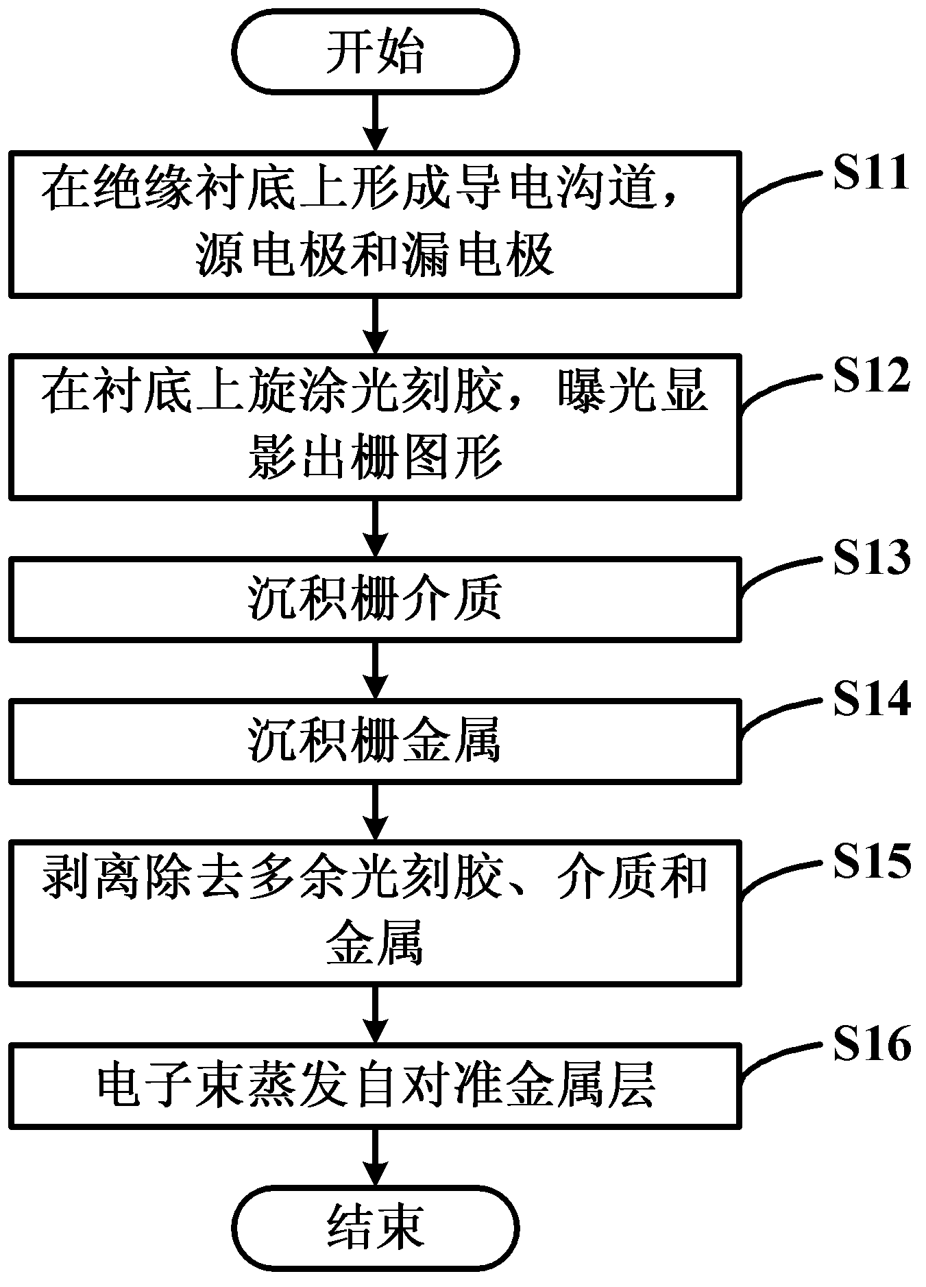
[0037] In order to make the object, technical solution and advantages of the present invention clearer, the present invention will be described in further detail below in conjunction with specific embodiments and with reference to the accompanying drawings.

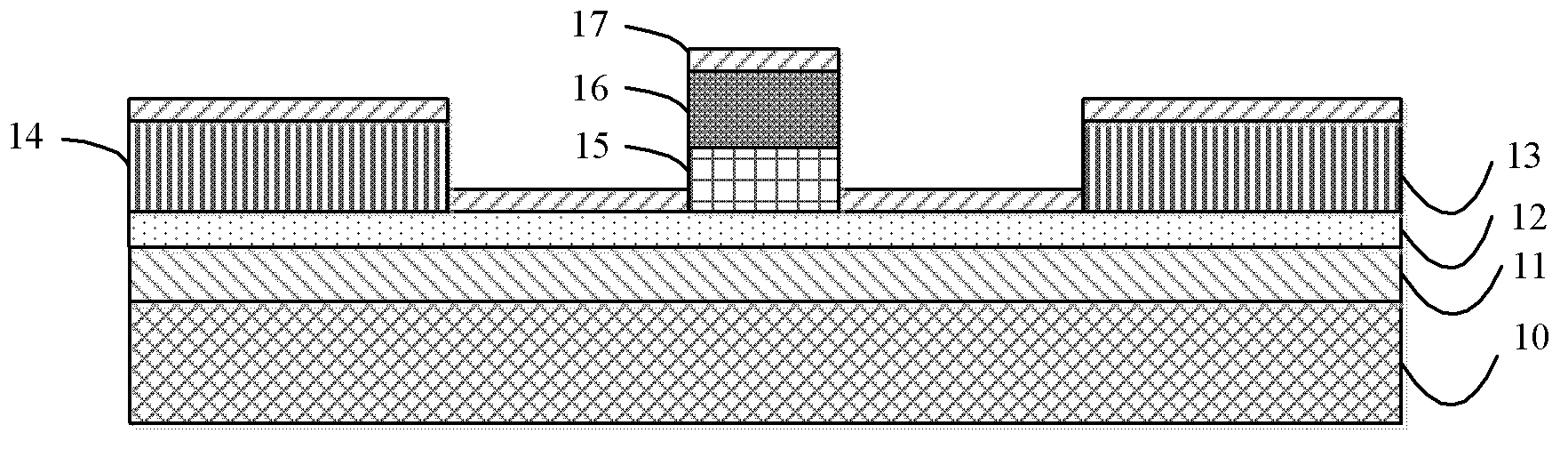
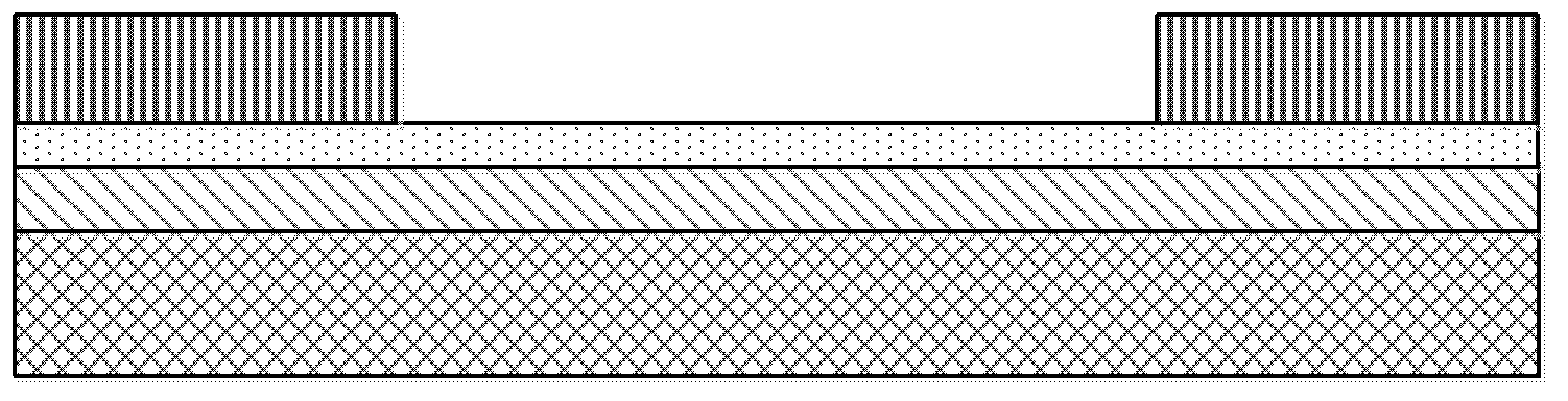
[0038] Such as figure 1 as shown, figure 1 is a schematic diagram of a self-aligned graphene field-effect transistor according to an embodiment of the present invention, and the self-aligned graphene field-effect transistor includes a semiconductor substrate 10, an insulating layer 11, a conductive channel 12, a source electrode 13, a drain electrode 14, a gate dielectric layer 15 , gate metal 16 and self-aligned metal 17 . Wherein, the insulating layer 11 is formed on the semiconductor substrate 10, the conductive channel 12 is formed on the insulating layer 11, the conductive channel 12 is made of graphene, and the source electrode 13 and the drain electrode 14 are respectively formed on both sides of the conductive ch...


PUM

PropertyMeasurementUnit
Thicknessaaaaaaaaaa
Thicknessaaaaaaaaaa

Abstract

The invention discloses a self-aligned graphene field effect transistor and a manufacturing method thereof. The self-aligned graphene field effect transistor comprises a semiconductor substrate, an insulating layer, a conducting channel, a source electrode, a drain electrode, a gate dielectric layer, gate metal, self-aligned metal, the insulating layer is formed on the semiconductor substrate, the conducting channel is is formed on an insulator and formed by graphene, the source electrode and the drain electrode are formed on two sides of the conducting channel respectively, the gate dielectric layer selectively deposits on the conducting channel between the source electrode and the drain electrode, the gate metal is formed on the gate dielectric layer, and the gate dielectric layer and the gate metal are simultaneously and graphically piled together to form a gate accumulation layer to control carrier concentration of a channel area. A self-aligned metal layer covers on the source electrode, the drain electrode, the conducting channel and the gate metal, so that the area of a region not being covered by a grid and self-aligning of a device grid and the source electrode as well as the drain electrode is realized.

Description

technical field [0001] The invention belongs to the technical field of field-effect transistor manufacturing, and in particular relates to a self-aligned graphene field-effect transistor and a preparation method thereof. Background technique [0002] Nanoelectronics based on carbon materials, especially graphene (Graphene) material, due to its high carrier mobility and saturation velocity, and its two-dimensional planar structure can be integrated with the traditional Si process, it is considered to have It has great application prospects and is considered to be a new material for the next generation of integrated circuits that can replace silicon. Since graphene was successfully developed in 2004, research on graphene devices has made great progress. Graphene-based micro-nano electronic devices have the characteristics of small size, fast speed, low power consumption, and simple process, and have attracted more and more attention. [0003] Graphene field-effect transistor...

Claims


Application Information

Patent Timeline
IPC IPC(8): H01L29/16H01L29/772H01L21/32H01L21/335
Inventor 金智彭松昂麻芃张大勇史敬元陈娇
Owner INST OF MICROELECTRONICS CHINESE ACAD OF SCI
Why Eureka
Try Eureka